Production method for semiconductor wafer

A manufacturing method and semiconductor technology, applied in semiconductor/solid-state device manufacturing, manufacturing tools, and machine tools suitable for grinding workpiece planes, etc., can solve the problems of slow cutting speed and inability to obtain wafer flatness, etc., to maintain wafer flatness , Omit the polishing process and reverse surface grinding process, the effect of small grinding damage

Inactive Publication Date: 2006-06-28
SUMCO CORP
View PDF1 Cites 4 Cited by
  • Summary
  • Abstract
  • Description
  • Claims
  • Application Information

AI Technical Summary

Problems solved by technology

However, abrasive particles act gently to obtain a wafer surface with less abrasive damage compared to a metal surface plate, but this method has problems that its cutting rate is slow, and the elastic surface plate wears quickly so that it cannot be obtained good wafer flatness

Method used


Image

  • Production method for semiconductor wafer
  • Production method for semiconductor wafer
  • Production method for semiconductor wafer

Examples


example

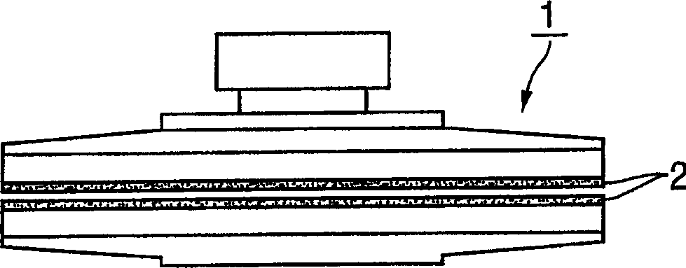
[0032] A slurry of GC#800 abrasive particles at a concentration of 0.3 wt% was supplied to a double-sided polisher with a porous closed-cell polyurethane pad ( image 3 ), and perform semi-fixed abrasive grinding. As a result, in a 300 mm wafer, a semiconductor wafer with a semi-specular surface, cutting rate = 2 to 5 μm / min, flatness TTV < 1.0 μm, and surface roughness Ra < 400 angstroms was obtained.

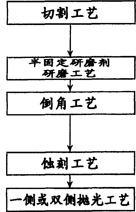
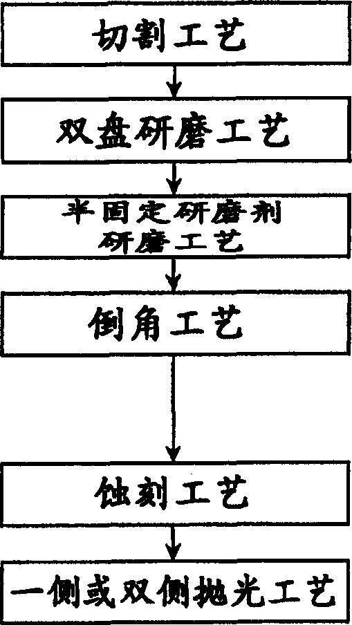
[0033] In addition, this process method (semi-fixed abrasive grinding) can be suitably combined with the manufacturing process steps shown in FIGS. 1 and 2 to manufacture semiconductor wafers. shown in Table 1 compared to Figure 7The conventional manufacturing process reduces the thickness of the removed part and results in microscopic surface relief (nanotopography).

[0034] As can be clearly seen from Table 1, compared to the conventional process ( Figure 7 ) in 10mm 2 Dimensions in the nanotopography value of 24.9nm, in figure 1 The fabrication process shown is 24....


PUM

PropertyMeasurementUnit
diameteraaaaaaaaaa
diameteraaaaaaaaaa

Abstract

The present invention provides a method of manufacturing a semiconductor wafer in which semi-fixed abrasive particle grinding with free abrasive particles reduces minute surface fluctuations caused by wire saw cutting or double disc grinding, while simplifying the manufacturing process of conventional semiconductor wafers step. A method of manufacturing a semiconductor wafer is characterized in that the following processes are performed: dicing, followed by chamfering, etching, and one-sided or two-sided polishing, wherein semi-fixation with porous polishing pads and free abrasive particles is performed after the dicing process Abrasive grinding process.

Description

technical field [0001] The present invention relates to a method for obtaining a semiconductor wafer from a single crystal ingot having high flatness and low processing distortion, and more particularly to a method for manufacturing such a semiconductor wafer by using a free abrasive The semi-fixed abrasive grinding of the particles reduces microscopic surface relief produced by wire saw dicing or double disc grinding, while planarizing the semiconductor wafer and simplifying conventional semiconductor wafer manufacturing process steps. Background technique [0002] Generally, a method of manufacturing a semiconductor wafer employs the following process steps: [0003] 1) A dicing process of dicing a single crystal ingot taken from a single crystal growth apparatus to obtain a thin disk-shaped wafer. [0004] 2) Chamfering process to prevent chips from chipping and cracking. [0005] 3) Polishing process to planarize the chamfered wafer. [0006] 4) Etching process to rem...

Claims


Application Information

Patent Timeline
Patent Type & Authority Applications(China)
IPC IPC(8): H01L21/304B24B7/17B24B9/06B24B37/00B24D13/14H01L21/306
CPCB24B7/17B24B9/065B24B37/042B24B37/08B24B37/245H01L21/02008H01L21/02013H01L21/30625H01L21/304H01L21/30
Inventor 浅川庆一郎
Owner SUMCO CORP
Why Eureka
Try Eureka