

Method for preparing thin film material of metal zirconium
A thin film material, metal zirconium technology, applied in metal material coating process, ion implantation plating, coating and other directions, can solve the problem of reducing the internal stress of metal zirconium thin film film, increasing contact resistance, affecting the quality of film growth, etc. problems, to achieve the effect of high-purity growth and reduction of raw material costs
- Summary
- Abstract
- Description
- Claims
- Application Information
AI Technical Summary
Problems solved by technology
Method used
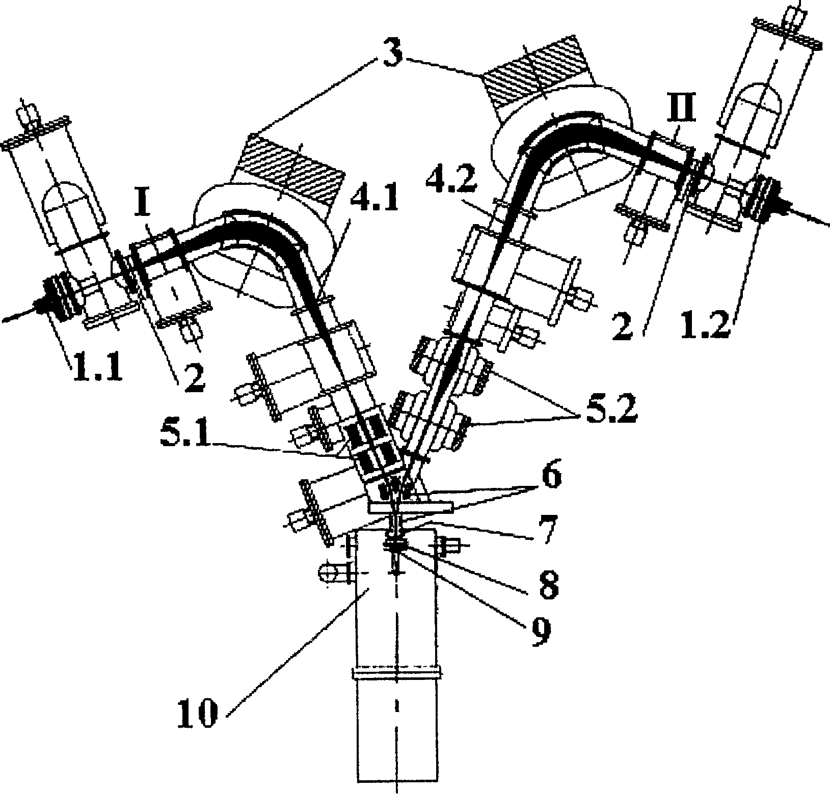
Image

Examples
Embodiment
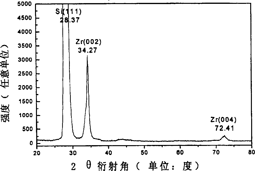
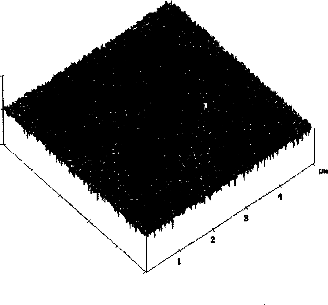
[0095] Concrete embodiment sees the relevant experimental data of table 1 and figure 2 , 3 , 4 experimental results.
[0096] Table 1: Experimental parameters and results of metal zirconium thin film materials prepared on silicon Si substrates using ion beam epitaxy (IBE) growth equipment.
[0097]
[0098]
[0099] V 离子束加速电压
15KV
15KV
15KV
V 磁分析器测谱电压
362.2mV
211.4mV
529.4mV
I 分析器后法拉第筒束流
3mA
2mA
0.1mA
V I束电四极透镜纵向电压
1.8KV
V I束电四极透镜横向电压
1.5KV
V II束磁四极透镜纵向电压
413mV
218mV
V II束磁四极透镜横向电压
341mV
181mV
V 静电偏转电极(正负)电压
1.7KV
1.6KV
1.6KV
V 减速透镜电压
300V
200V
200V
I 靶面束流
400μA
300μA
30μA
Argon ions (Ar + ) beam dry cleani...
PUM
 Abstract
Description
Claims
Application Information