Method for fabricating transistor of single electron based on Nano carbon tubes

A technology of single-electron transistors and carbon nanotubes, applied in nanostructure manufacturing, nanotechnology, nanotechnology, etc., can solve problems such as reducing tunnel junction capacitance and reducing electrode size

Inactive Publication Date: 2006-07-05
PEKING UNIV
View PDF0 Cites 8 Cited by
  • Summary
  • Abstract
  • Description
  • Claims
  • Application Information

AI Technical Summary

Problems solved by technology

[0004] Aiming at the problems existing in the electrode size and materials of current single-electron transistors, the present invention proposes to use carbon nanotubes as nano-electrodes to replace metal material electro

Method used


Image

  • Method for fabricating transistor of single electron based on Nano carbon tubes
  • Method for fabricating transistor of single electron based on Nano carbon tubes

Examples


Embodiment Construction

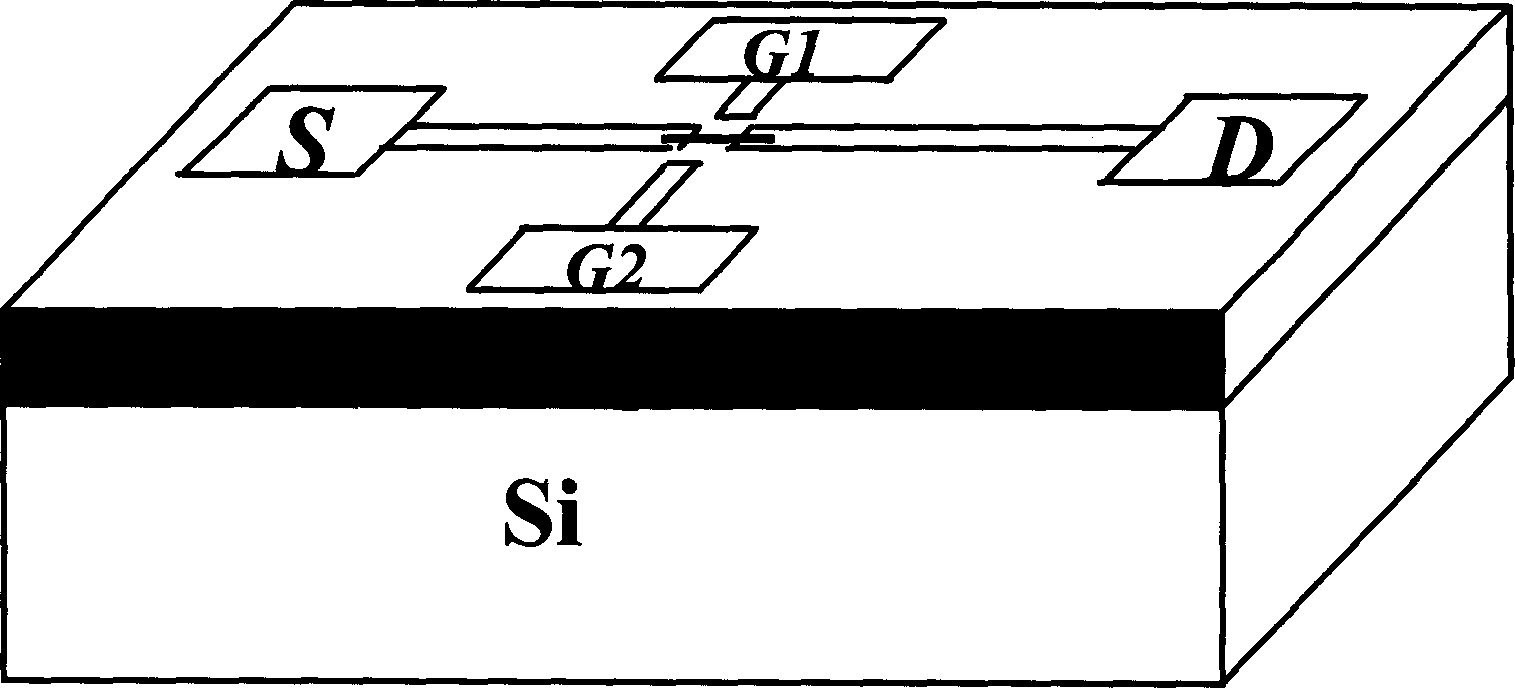
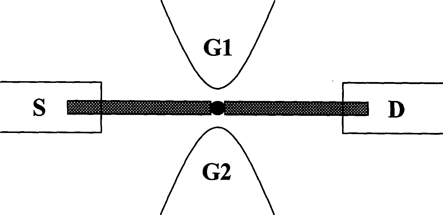
[0021] 1. Electrode design and preparation

[0022] In order to prepare nano-electrode pairs of carbon nanotubes (or tube bundles), first design micron-scale metal electrodes, the electrode shape is cross-shaped, the design width is 2 μm, the distance between opposite electrodes is 2 μm, and the distance between adjacent electrodes is 200-500nm. On the P-type heavily doped silicon substrate, silicon dioxide with a thickness of 180-300nm is thermally oxidized and grown as an insulating layer, and the metal electrode is prepared by photolithography and lift-off process. The process is: photolithography, exposure, and development; Then, the metal is deposited by sputtering, and the glue is removed to obtain a metal electrode. The electrode material is Ti / Au (10nm / 100nm). The schematic diagram of metal electrode and single electron device structure is attached figure 1 shown.

[0023] 2. Lap carbon nanotubes (or tube bundles) on metal electrodes

[0024] A pair of opposite elec...


PUM

PropertyMeasurementUnit
Sizeaaaaaaaaaa

Abstract

The method includes steps: first preparing a cross type metal electrodes in micro scale; using a piece of Nano carbon tube (or tube bundle) to lap a selected opposite pair of metal electrode; gap size smaller than 3 Nano generated on Nano carbon tube (or tube bundle) forms a pair of electrode; trapping single organic or inorganic molecule (or granule) in the gap; finally, using another pair of metal electrode in the cross type metal electrodes as dual gate electrode so as to form transistor of single electron. The method can solve interactional issue between metal electrodes and molecules as well as reduce capacitance of tunnel junction effectively so that the invention makes device possible to operate under room temperature.

Description

technical field [0001] The invention belongs to the field of research and development of single-electron transistors, and in particular relates to a method for preparing a single-electron transistor based on carbon nanotubes. Background technique [0002] The single-electron transistor is an important discovery in microelectronics science. As the traditional MOSFET is scaled down to the nanometer scale, more and more attention has been paid to the single-electron device. Its outstanding advantages of high speed and low power consumption make it in the future It has a wide range of application prospects in integrated circuits, and may even become an ideal construction of molecular computers in the future. [0003] The main structure of a single-electron transistor consists of Coulomb islands (quantum dots) surrounded by two tunnel junctions. The key to fabricating single-electron devices is how to control the Coulomb island size or the gap size between electrode pairs. At p...

Claims


Application Information

Patent Timeline
IPC IPC(8): H01L21/336H01L21/28B82B3/00
Inventor 郭奥傅云义刘佳黄如张兴
Owner PEKING UNIV
Why Eureka
Try Eureka