Gas sensor of hydrogen semiconductor transducer, and preparation method

The technology of a gas sensor and its manufacturing method is applied in the direction of electrical components, electrical solid devices, circuits, etc., and can solve the problems of not being able to meet the needs of real-time monitoring of hydrogen leakage, poor selectivity and sensitivity, etc., and achieve good consistency and low price , good selective effect

Active Publication Date: 2006-07-05
GRIMAT ENG INST CO LTD
View PDF0 Cites 14 Cited by
  • Summary
  • Abstract
  • Description
  • Claims
  • Application Information

AI Technical Summary

Problems solved by technology

[0003] As we all know, hydrogen is a renewable and clean energy source with no pollution and renewable energy. With the shortage of fossil fuels and the development of the microelectronics industry, hydrogen is used more and more frequently in daily life, but the concentration of hydrogen in the air reaches 4.1% to 75.6

Method used


Image

  • Gas sensor of hydrogen semiconductor transducer, and preparation method
  • Gas sensor of hydrogen semiconductor transducer, and preparation method
  • Gas sensor of hydrogen semiconductor transducer, and preparation method

Examples


Embodiment 1

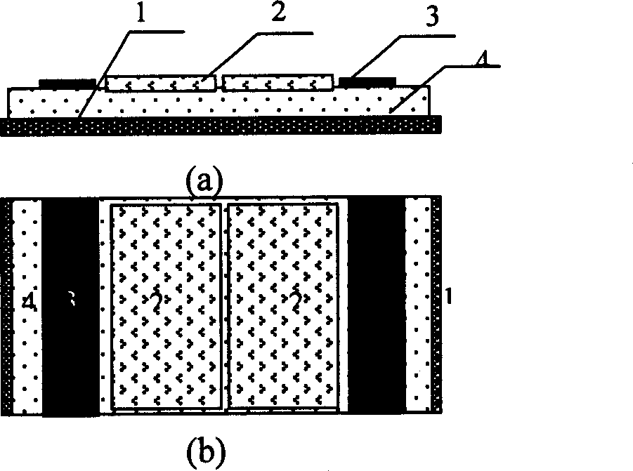
[0033] Firstly, the tin dioxide micropowder is subjected to hot isostatic pressing, and the process is to dry the tin dioxide micropowder at 110°C for 18 hours, and then sinter at 1050°C for 4 hours.

[0034] Then carry out surface treatment to the Si single wafer of (100) plane, and its process is to use H to treat the Si single wafer of (100) plane 2 SO 4 +K 2 Cr 2 o 7 Soak in the lotion for 24 hours, and then use methanol, acetone, and ethanol as media to ultrasonically clean the soaked silicon wafers to obtain a clean silicon substrate.

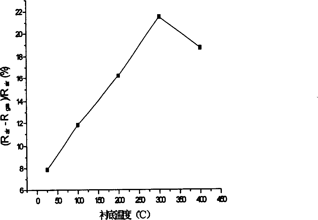
[0035] Then prepare a tin dioxide semiconductor thin film, and carry out radio frequency sputtering on a tin dioxide target with a sintered density of 90%. Sputtering parameters: sputtering power 65W; sputtering time 15 minutes; substrate temperature 25°C; P O2 / P Ar It is 1:4. The in-situ annealing process of the tin dioxide thin film is 400° C. for 6 hours. A Cu electrode was deposited on the prepared tin dioxide film, and then a...

Embodiment 2

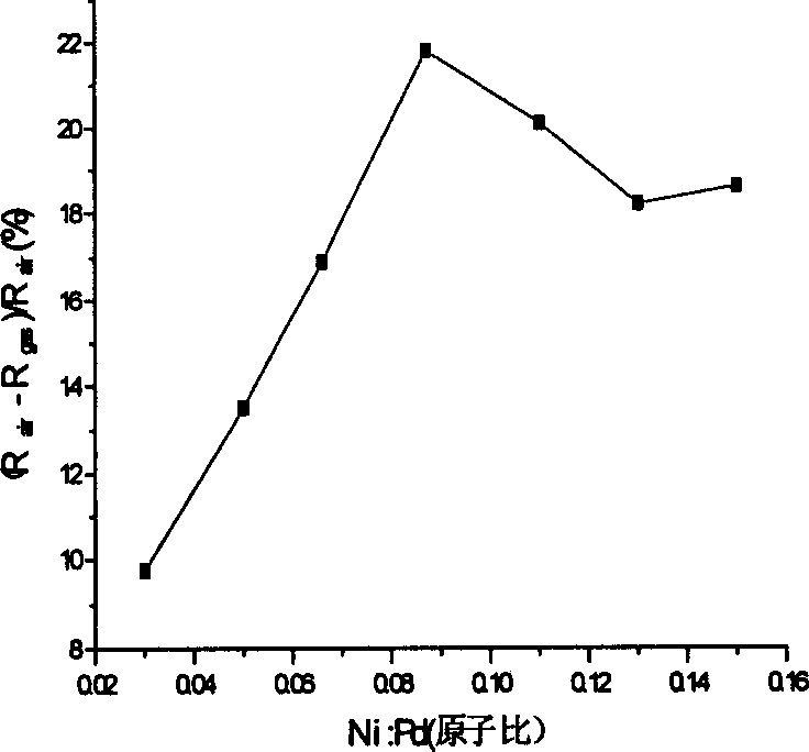
[0036] Embodiment 2: Except that the preparation process parameters of the tin dioxide thin film are different from that of Embodiment 1, the preparation methods adopted for each layer of Embodiment 2 are the same as those of Embodiment 1. The preparation process parameters of tin dioxide thin film are: sputtering power 98W; sputtering time 15 minutes; substrate temperature 400 ℃; P O2 / P Ar It is 1:4. The in-situ annealing process of the tin dioxide thin film is 700° C. for 6 hours. Cu electrodes were deposited on the prepared tin dioxide film. Ni:Pd=0.1 (atomic ratio) in the Pd-Ni alloy thin film, the thickness is 47nm, and it is annealed at 650° C. for 5.5 hours. It is proved by XRD and XPS tests that the tin dioxide film is an N-type semiconductor film with obvious (211) preferred orientation.

[0037]When the semiconductor sensor gas sensor in the present invention is actually used, that is, when detecting in an environment containing hydrogen, the hydrogen molecules ...


PUM

PropertyMeasurementUnit
Thicknessaaaaaaaaaa

Abstract

Characters of the method are that n-SnO2-x thin membrane layer is prepared on Si(100) chip by using radio frequency sputtering technique; then, Pd-Ni layer is prepared on tin dioxide layer so as to form gas sensor in composite membrane of Pd-Ni/SnO2. Under environment of normal temperature, the gas sensor raises selectivity and sensibility for hydrogen. Features are: simple technique and low cost.

Description

technical field [0001] The invention relates to a semiconductor sensor sensitive element sensitive to hydrogen and a manufacturing method thereof, and belongs to the technical field of semiconductor sensor gas sensor manufacturing technology. Background technique [0002] Semiconductor gas sensor refers to the use of semiconductor materials as sensitive elements, and the corresponding selectivity and sensitivity are improved by doping or surface modification technology. Due to the change of the ambient gas composition, the electrical properties of the semiconductor gas sensor change, and the type and concentration of the gas present in the environment are detected by measuring the surface resistance of the semiconductor gas sensor. [0003] As we all know, hydrogen is a renewable and clean energy source with no pollution and renewable energy. With the shortage of fossil fuels and the development of the microelectronics industry, hydrogen is used more and more frequently in d...

Claims


Application Information

Patent Timeline
IPC IPC(8): H01L49/00G01N27/12
Inventor 王磊熊玉华杜军毛昌辉尉秀英杨志民秦光荣苑鹏
Owner GRIMAT ENG INST CO LTD
Why Eureka
Try Eureka