Semiconductive chip device having insulating coating layer and method of manufacturing the same

An insulating coating, semiconductor technology, applied in the direction of semiconductor devices, semiconductor devices, semiconductor/solid-state device components of light-emitting elements, etc., can solve the problems of complex technical process and unsuitable application, etc.

Inactive Publication Date: 2006-08-23
SAMSUNG ELECTRO MECHANICS CO LTD
View PDF2 Cites 2 Cited by
  • Summary
  • Abstract
  • Description
  • Claims
  • Application Information

AI Technical Summary

Problems solved by technology

However, the above-mentioned technical process is complicated, so it is contrary to the requirements of economic benefits and is not suitable for practical application.

Method used


Image

  • Semiconductive chip device having insulating coating layer and method of manufacturing the same
  • Semiconductive chip device having insulating coating layer and method of manufacturing the same
  • Semiconductive chip device having insulating coating layer and method of manufacturing the same

Examples


Embodiment Construction

[0022] The present invention will be described in detail below with reference to the accompanying drawings.

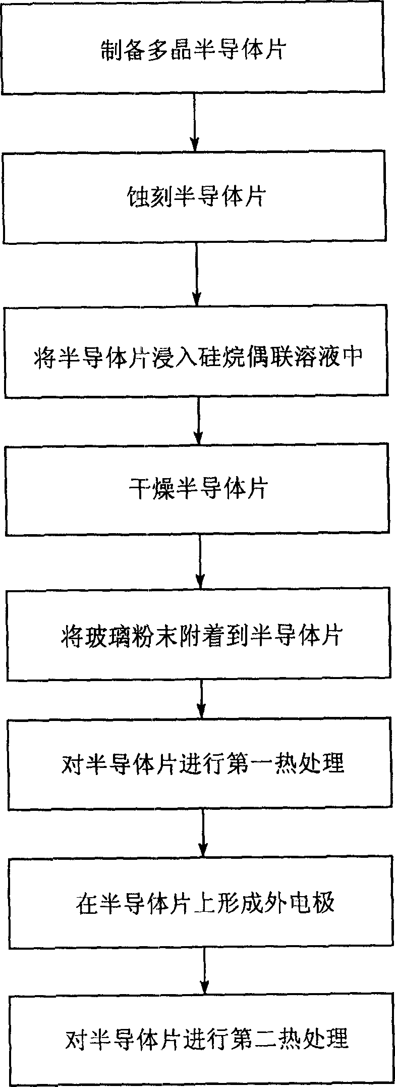
[0023] figure 2 The view in the figure shows the process of manufacturing a semiconductor chip device according to the present invention. Such as figure 2 As shown, a polycrystalline semiconductor wafer that requires surface insulation properties is first prepared. Polycrystalline semiconductor chips requiring surface insulating properties are applied to chip varistors, such as PTCR and MTCR, etc., but not limited to these.

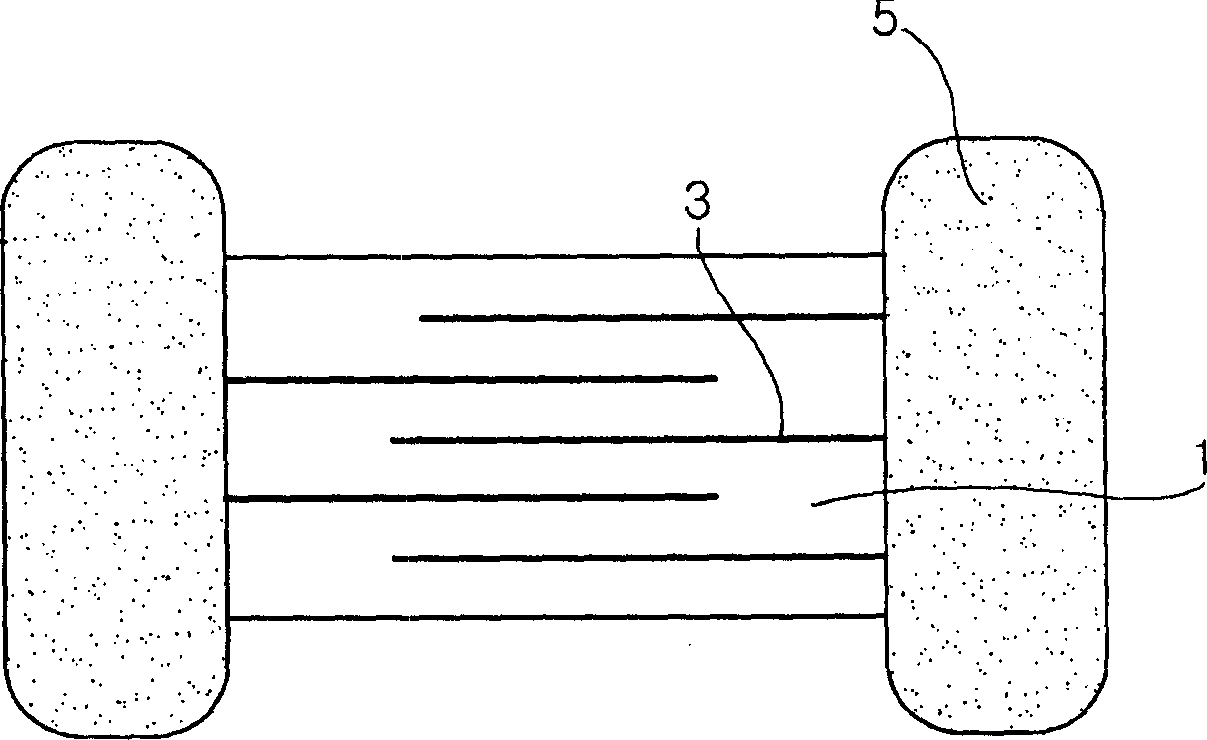
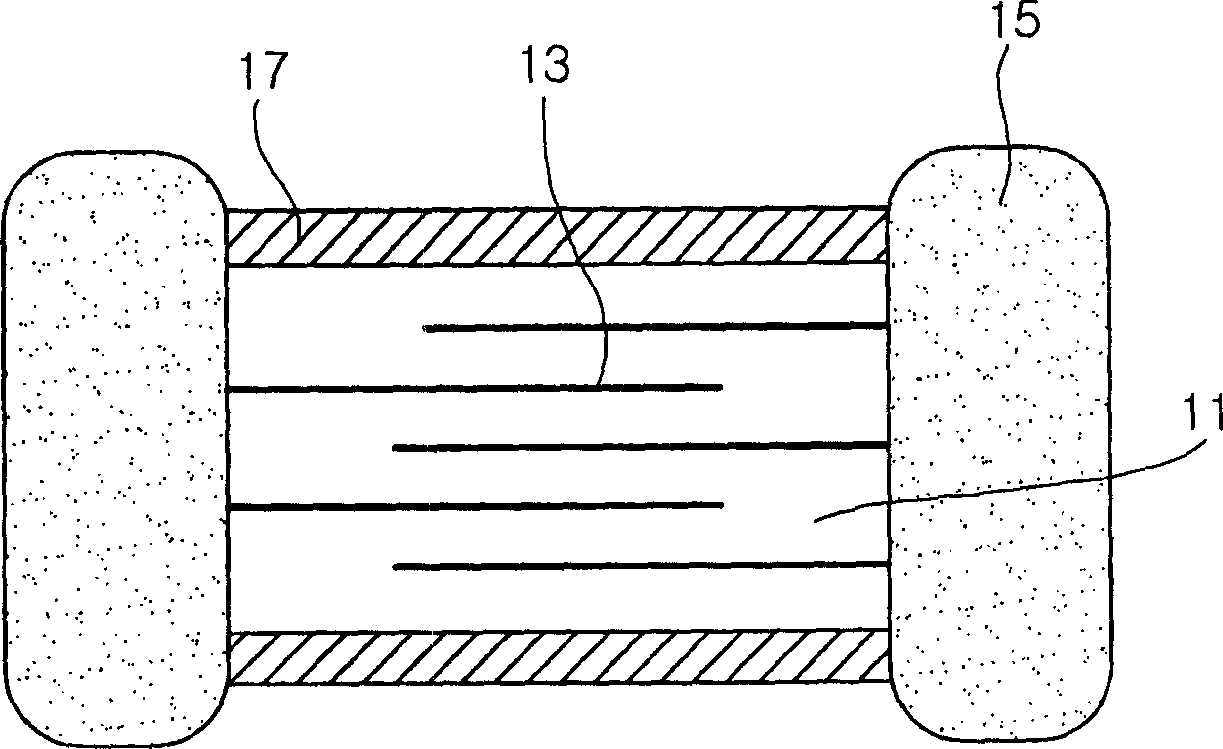
[0024] Polycrystalline semiconductor wafers are mainly classified into a laminated type and a disk type, each of which can be used in the present invention. see Figure 1b , the laminated semiconductor chip is formed as a semiconducting ceramic laminate, including dielectric layers 11 and internal electrodes 13 sandwiched between the dielectric layers 11 and alternately connected to both ends of the dielectric layer 11 . At this time, the d...


PUM


Abstract

Disclosed herein is a semiconductive chip device having an insulating coating layer, which includes a multi-crystalline semiconductive chip requiring surface insulation properties, outer electrodes formed at both ends of the semiconductive chip, and an insulating coating layer formed by fusing glass powder to a silane coupling agent on the surface of the semiconductive chip. In addition, a method of manufacturing the semiconductive chip device having an insulating coating layer is provided, which comprises: preparing a multi-crystalline semiconductive chip requiring surface insulation properties, and etching the multi-crystalline semiconductive chip; dipping the etched semiconductive chip into a silane coupling solution, and removing the aqueous component from the solution attached to the surface of the semiconductive chip; attaching glass powder to the surface of the semiconductive chip having no aqueous component, and primarily heat treating the semiconductive chip; and forming outer electrodes on the primarily heat treated semiconductive chip, and, secondarily heat treating the semiconductive chip, thereby forming the insulating coating layer on the surface of the semiconductive chip.

Description

technical field [0001] The present invention generally relates to semiconductor chip devices having an insulating coating thereon and methods of making the same. More specifically, the present invention relates to a semiconductor chip device on which an insulating coating is formed to effectively prevent flux erosion when performing a subsequent reflow process, thereby maintaining the original insulation resistance. The present invention also relates to this Method for semiconductor chip devices. Background technique [0002] Recently, various electronic devices such as mobile communication terminals have been miniaturized, and at this time, miniaturization and high integration of circuit elements used in the electronic devices are required. Accordingly, circuit components have been designed to have low voltage and current ratings. [0003] A typical representative of the above-mentioned elements, a varistor is a device that significantly exhibits a nonlinear voltage-curre...

Claims


Application Information

Patent Timeline
Patent Type & Authority Applications(China)
IPC IPC(8): H01C7/00H01C17/00
CPCH01G2/12H01L2924/3011H01G4/30H01C1/028H01G4/232H01C7/001H01C17/02H01C7/18H01L2924/0002H01G4/255H01L2924/09701H01L23/291H01L2924/00G09B23/183F21K9/00
Inventor 高敬憙申知桓崔畅学
Owner SAMSUNG ELECTRO MECHANICS CO LTD
Why Eureka
Try Eureka