Use of copper Dimashg process in production of integrated circuits

A back-end process and integrated circuit technology, which is applied in the manufacturing field using the copper damascene back-end process, can solve the problems of metal/insulating medium corrosion, copper metal wire metal/insulating medium corrosion, etc., so as to reduce adverse reactions and improve the quality of finished products. rate effect

Inactive Publication Date: 2006-11-01
SHANGHAI INTEGRATED CIRCUIT RES & DEV CENT +2
View PDF0 Cites 7 Cited by
  • Summary
  • Abstract
  • Description
  • Claims
  • Application Information

AI Technical Summary

Problems solved by technology

[0012] However, since each layer of Damascus will use metal chemical mechanical polishing twice (copper chemical mechanical polishing and tantalum nitride/tantalum metal layer chemical mechanical polishing), multiple polishing and to ensure that there is no residual copper and barrier metal between metal connections The over-polishing process will bring considerable negative effects, leading to adverse reactions of copper metal wire depression (Disshing) and metal/insulation medium corrosion (Erosion), and especially in

Method used


Image

  • Use of copper Dimashg process in production of integrated circuits
  • Use of copper Dimashg process in production of integrated circuits
  • Use of copper Dimashg process in production of integrated circuits

Examples


Embodiment Construction

[0031] Now in conjunction with accompanying drawing, the specific embodiment of the present invention is described in further detail:

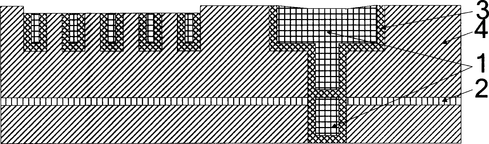
[0032] First, if Figure 2A as shown ( Figure 2A For the schematic diagram of the completed Damascus topography process), complete the Damascus topography process.

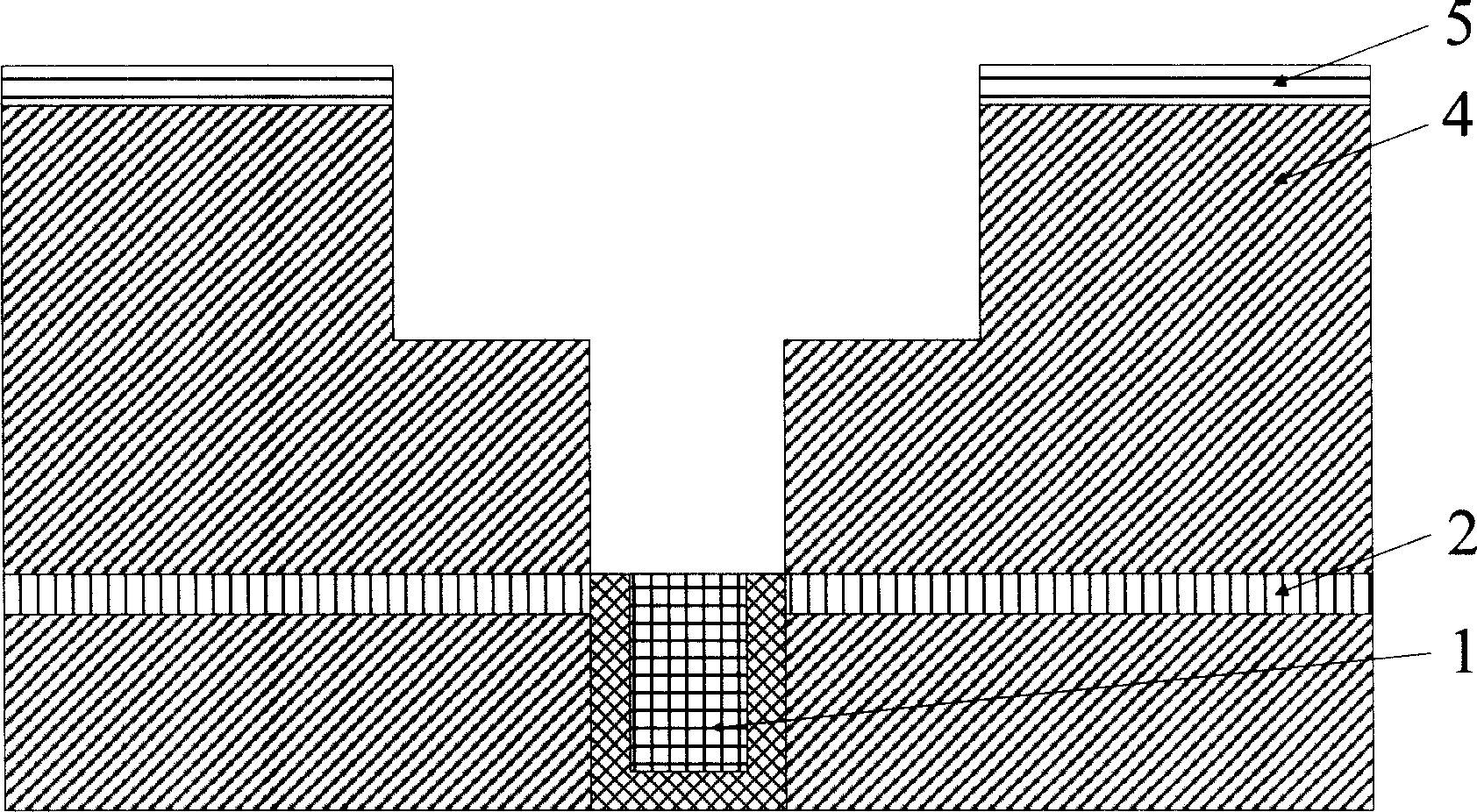
[0033] Secondly, if Figure 2B as shown ( Figure 2B It is a schematic diagram of physical vapor deposition of a tantalum nitride / tantalum metal layer), and a physical vapor deposition of a tantalum nitride / tantalum metal layer on the top etch barrier layer, the damascene dielectric layer, and the bottom copper metal layer.

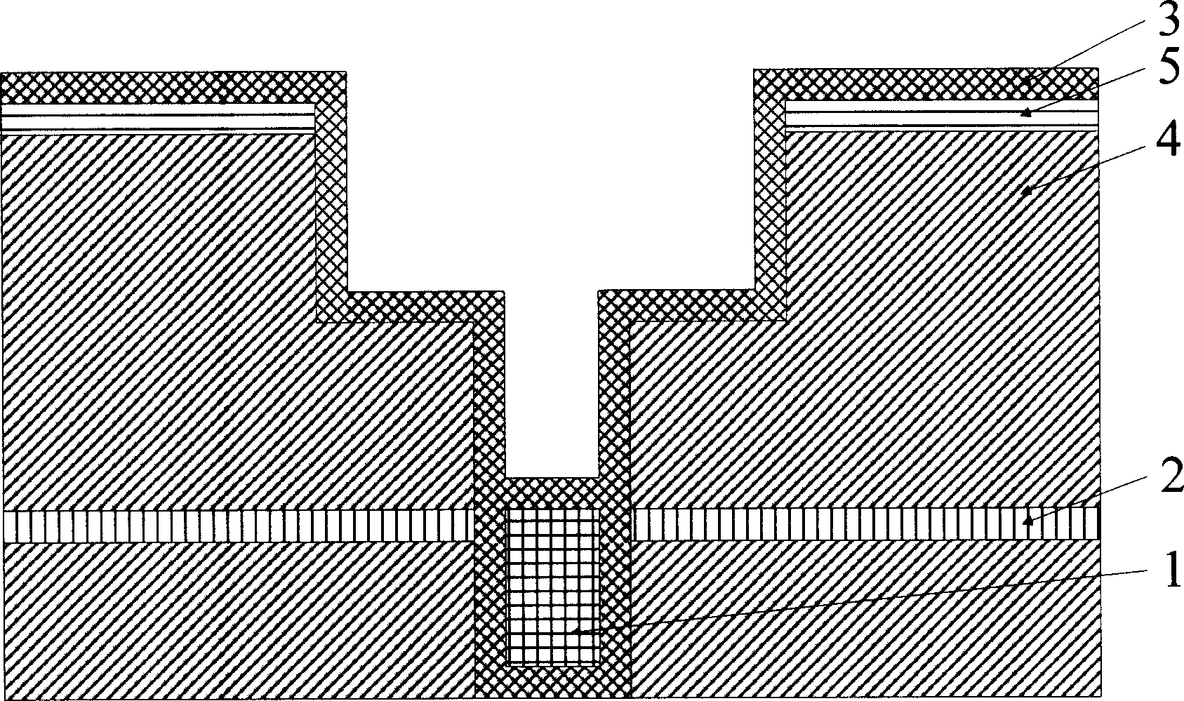
[0034] Secondly, if Figure 2C as shown ( Figure 2C For the schematic diagram of coating the bottom anti-reflection absorption material), the photosensitive material flat surface process is carried out, that is, the bottom anti-reflection absorption material is coated on the tantalum nitride / tantalum metal layer, filled with damascene patterns, and bak...


PUM

PropertyMeasurementUnit
Surface flatnessaaaaaaaaaa

Abstract

The method comprises: based on the flat surface of photosensitive material and the polysilicon etch-back technology, a selective etch is made for the tantalum nitride and tantalum metal layer deposited with physical vapour deposition process; a one time metal copper chemical mechanical polishing is used to replace the original two times polishing process, copper chemical mechanical polishing and tantalum nitride/tantalum metal layer polishing. The invention reduces the dishing of metal wire and the erosion of insulation media caused by over-polishing from multi times of chemical mechanical polishing.

Description

technical field [0001] The invention belongs to the field of integrated circuit manufacturing technology, and in particular relates to a manufacturing method using copper damascene back-end technology in integrated circuit production. Background technique [0002] With the continuous improvement of integrated circuit manufacturing technology, the volume of semiconductor devices is becoming smaller and smaller, which makes the parasitic capacitance between metals more and more large. For microprocessors, the chip speed is mainly limited by the resistance and Parasitic capacitance is generated. As a result, problems such as resistance-capacitance time delay, mutual interference between signals, and energy loss have become increasingly prominent. In order to solve the problem of resistance-capacitance time delay, the industry's response has always been to use low-dielectric materials (dielectric constant 2.0 to 4.0), so that the dielectric constant of the dielectric layer betw...

Claims


Application Information

Patent Timeline
IPC IPC(8): H01L21/768H01L21/3205H01L21/321H01L21/3213
Inventor 朱骏方精询缪炳有
Owner SHANGHAI INTEGRATED CIRCUIT RES & DEV CENT
Why Eureka
Try Eureka