

Photoelectric conversion device
A technology of photoelectric conversion device and conductive substrate, applied in photovoltaic power generation, circuits, electrical components, etc., can solve the problem of low short-circuit current density and other problems
- Summary
- Abstract
- Description
- Claims
- Application Information
AI Technical Summary
Problems solved by technology
Method used
Image

Examples
example 1
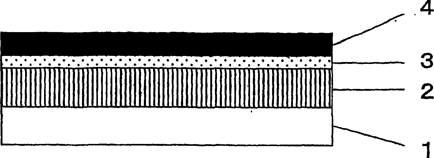
[0064] The dye-sensitized photoelectric conversion device according to the present invention is fabricated through the following steps. First, a titanium substrate having a size of 5×5 cm and a thickness of 1 mm was prepared, and an epoxy resin mask was coated on one surface of the substrate. The other surfaces were polished by electropolishing the titanium substrate using a mixed solution of methanol and sulfuric acid. After electropolishing, the surface profile of the substrate was observed by AFM (Atomic Force Microscope), and it was confirmed that the substrate had a very smooth surface structure. The roughness factor of the substrate surface was 1.04.
[0065] The titanium substrate was then anodized by applying a voltage of 10 V for 30 minutes in an electrolytic aqueous solution containing 0.5% by mass of hydrofluoric acid, thereby forming a titanium oxide thin film on the substrate. The electrolytic solution was set at a temperature of 16 °C.
[0066] The substrate w...
example 2
[0071] The dye-sensitized photoelectric conversion device according to the present invention is fabricated through the following steps. First, a titanium substrate having a size of 5×5 cm and a thickness of 1 mm was prepared, and an epoxy resin mask was coated on one surface of the substrate. The other surfaces are planarized by electropolishing the titanium substrate using a mixed solution of methanol and sulfuric acid. After electropolishing, the surface profile of the substrate was observed by AFM (Atomic Force Microscope), and it was confirmed that the substrate had a very smooth surface structure. The roughness factor of the substrate surface was 1.04.
[0072] The titanium substrate was then anodized by applying a voltage of 20 V for 20 minutes in an electrolytic aqueous solution containing 0.5% by mass of hydrofluoric acid, thereby forming a titanium oxide thin film on the substrate. The electrolytic solution was set at a temperature of 16 °C.
[0073] The substrate ...
example 3
[0078] The dye-sensitized photoelectric conversion device according to the present invention is fabricated through the following steps. First, an ITO glass substrate with a size of 5×5 cm and a thickness of 3 mm was prepared, and titanium with a thickness of 1000 nm was superimposed on the ITO glass substrate by vacuum deposition. The surface profile of titanium was observed by AFM (Atomic Force Microscope), and it was confirmed that titanium had a very smooth surface structure. The roughness factor of the titanium surface is 1.02.
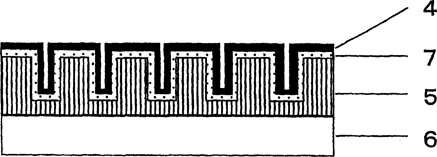
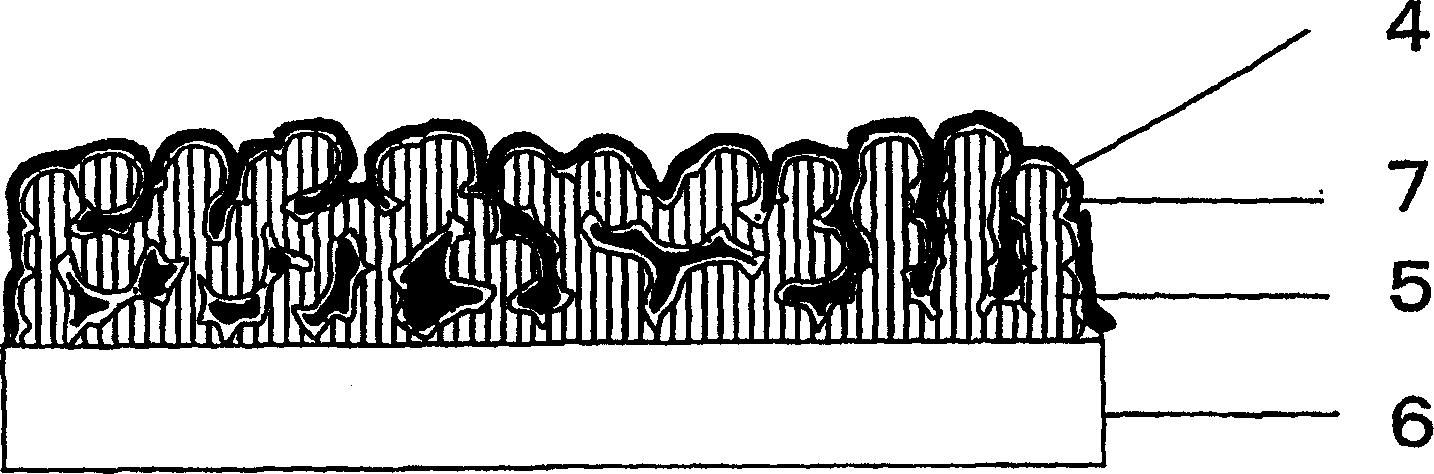
[0079] The deposited titanium is then anodized by constant current electrolysis in an aqueous solution containing 1.5 mol / l sulfuric acid and 0.3 mol / l hydrogen peroxide until the generated voltage reaches 150 V, thereby forming an oxide on the substrate. Titanium film. The current density and the temperature of the electrolytic solution were set at 30mA / cm 2 and 16°C. The thin film obtained in this way was a de-titanium type crystal, and had ...
PUM
| Property | Measurement | Unit |
|---|---|---|
| electrical conductivity | aaaaa | aaaaa |
| diameter | aaaaa | aaaaa |
| thickness | aaaaa | aaaaa |
Abstract
Description
Claims
Application Information