Method for preparing polysilicon in high purity in use for solar cell

A technology for solar cells and preparation devices, which is applied in the growth of polycrystalline materials, chemical instruments and methods, crystal growth, etc., can solve the problems of expensive electron beam equipment, and achieve fast and convenient smelting and impurity removal, low cost, and simple devices Effect

Inactive Publication Date: 2006-12-06
DALIAN UNIV OF TECH
View PDF1 Cites 32 Cited by
  • Summary
  • Abstract
  • Description
  • Claims
  • Application Information

AI Technical Summary

Problems solved by technology

However, electron beam equipment is expensive

Method used


Image

  • Method for preparing polysilicon in high purity in use for solar cell
  • Method for preparing polysilicon in high purity in use for solar cell

Examples


Embodiment 1

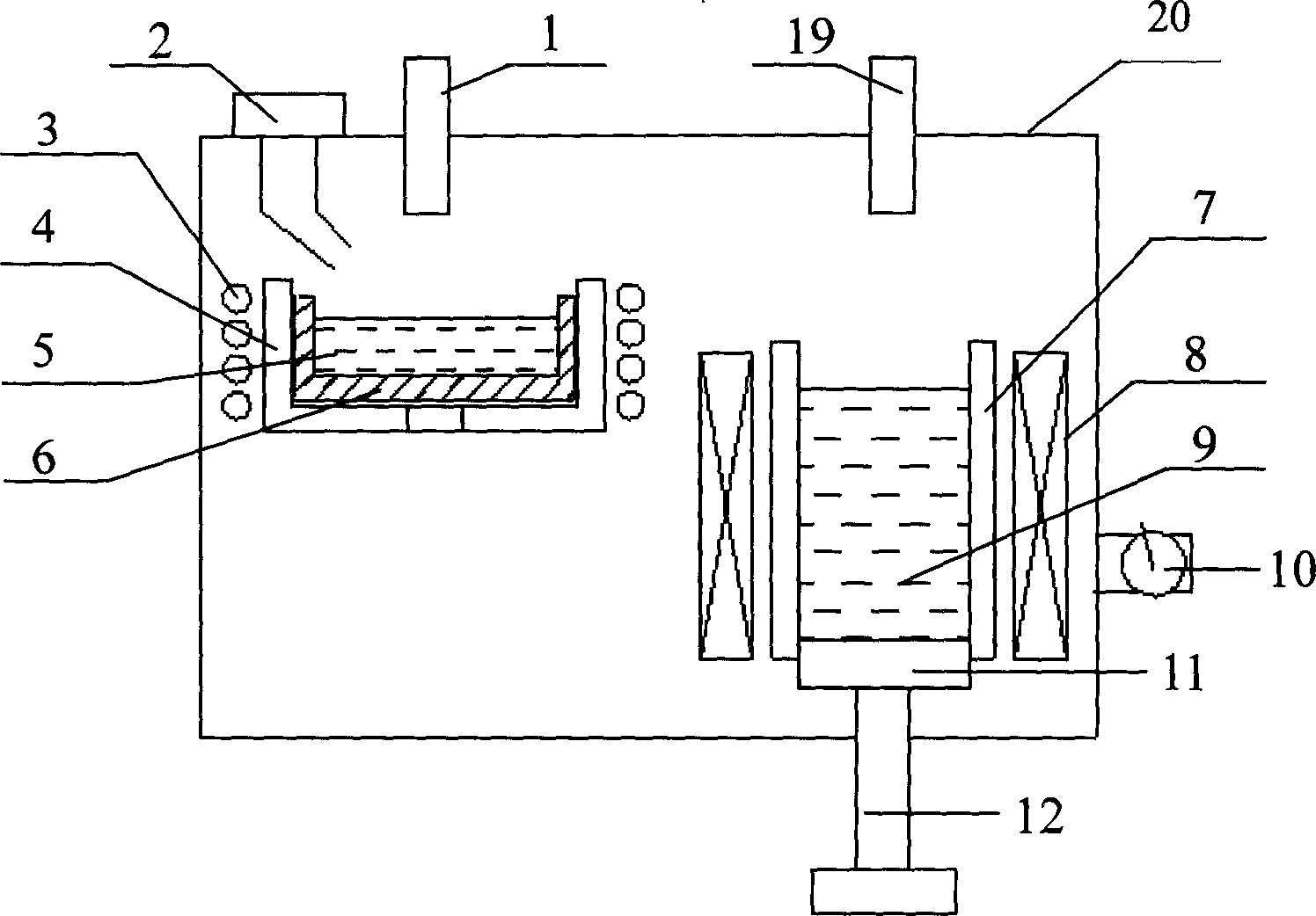
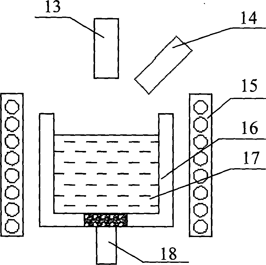
[0022] Put the industrial silicon 5 into the crucible 6, and the vacuum system is evacuated to 10 -2 After Pa, the electromagnetic induction heater 3 is turned on to melt the industrial silicon 5, and the power supply of the holding furnace 8 is turned on simultaneously. When the temperature of the silicon in the crucible 6 reaches 1500°C, keep it warm for 30-60 minutes, move the manipulator to pour the molten silicon into the directional solidification crucible 7, and use the holding furnace 8 to keep the temperature of the liquid silicon 9; then, start the casting system 12 , drive the directional solidification cooling bottom mold 11 to move downward at a speed of 5mm / min, and obtain a slab with a diameter of 160mm and a length of 250mm, and the silicon content is 99.99% through composition testing. Put the directionally solidified billet into the refining crucible 16 of the secondary purification device, use the secondary purification heating furnace 15 to melt and keep it...

Embodiment 2

[0024] Put the industrial silicon 5 into the crucible 6, and the vacuum system is evacuated to 10 -2 After Pa, the electromagnetic induction heater 3 and the plasma gun 1 are turned on to melt the industrial silicon 5, and the power supply of the holding furnace 8 is turned on simultaneously. When the temperature of the silicon in the crucible 6 reaches 1500°C, keep it warm for 30-60 minutes, pull the manipulator to pour the molten silicon into the directional solidification crucible 7, use the holding furnace 8 and the plasma gun 19 to keep the temperature of the liquid silicon 9; then, start The billet drawing system 12 drives the directional solidification cooling bottom mold 11 to move downward at a speed of 3mm / min to obtain a billet with a diameter of 160mm and a length of 250mm, and the silicon content is 99.99% according to the composition test. Put the directionally solidified billet into the refining crucible 16 of the secondary purification device, use the secondary...


PUM


Abstract

This invention discloses method and device for preparing high purity polycrystalline silicon for solar cells. This invention combines vacuum electromagnetic induction smelting, plasma oxidation and purification, and oriented-solidification to prepare high purity silicon ingots for solar cells. The method comprises: (1) applying an alternative electromagnetic field (Q is J2 / sigma) at the outer side of solid silicon according to electromagnetic theory; (2) smelting to remove impurities such as P in liquid silicon according to chemical equilibrium theory; (3) performing oriented-solidification according to metal solidification theory that the elements whose equilibrium distribution coefficients are less than 1 can be enriched at the last solidification site, and thus discharged from the liquid. This invention has such advantages as simple equipment, rapid and convenient smelting and purification, uniform solidification, no cracking, no segregation.

Description

technical field [0001] The invention belongs to the technical field of semiconductor material preparation. In particular, it relates to a production technology for producing high-purity polycrystalline silicon wafers for solar cells by using industrial silicon as a raw material through a series of metallurgical methods. Background technique [0002] Solar energy has become the preferred energy source to solve the energy crisis and environmental degradation due to its wide distribution, cleanliness and non-pollution. Therefore, research on high-efficiency and low-cost solar cells has attracted worldwide attention. Today's solar cells include silicon solar cells, compound solar cells, nanocrystalline fuel-sensitized cells, and organic solar cells. Silicon solar cells have become mainstream products due to their rich silicon material resources, non-toxic and harmless, and excellent physical properties. [0003] Silicon solar cells are divided into monocrystalline silicon sola...

Claims


Application Information

Patent Timeline
Patent Type & Authority Applications(China)
IPC IPC(8): C30B29/06C30B28/06
Inventor 李廷举
Owner DALIAN UNIV OF TECH
Why Eureka
Try Eureka