

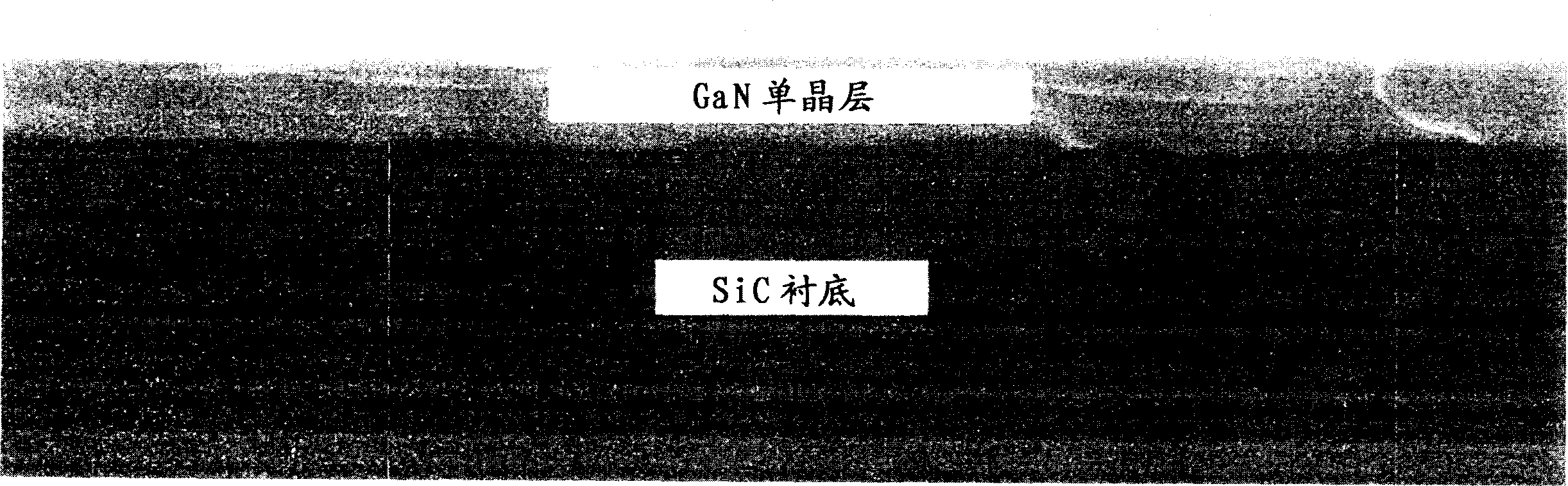
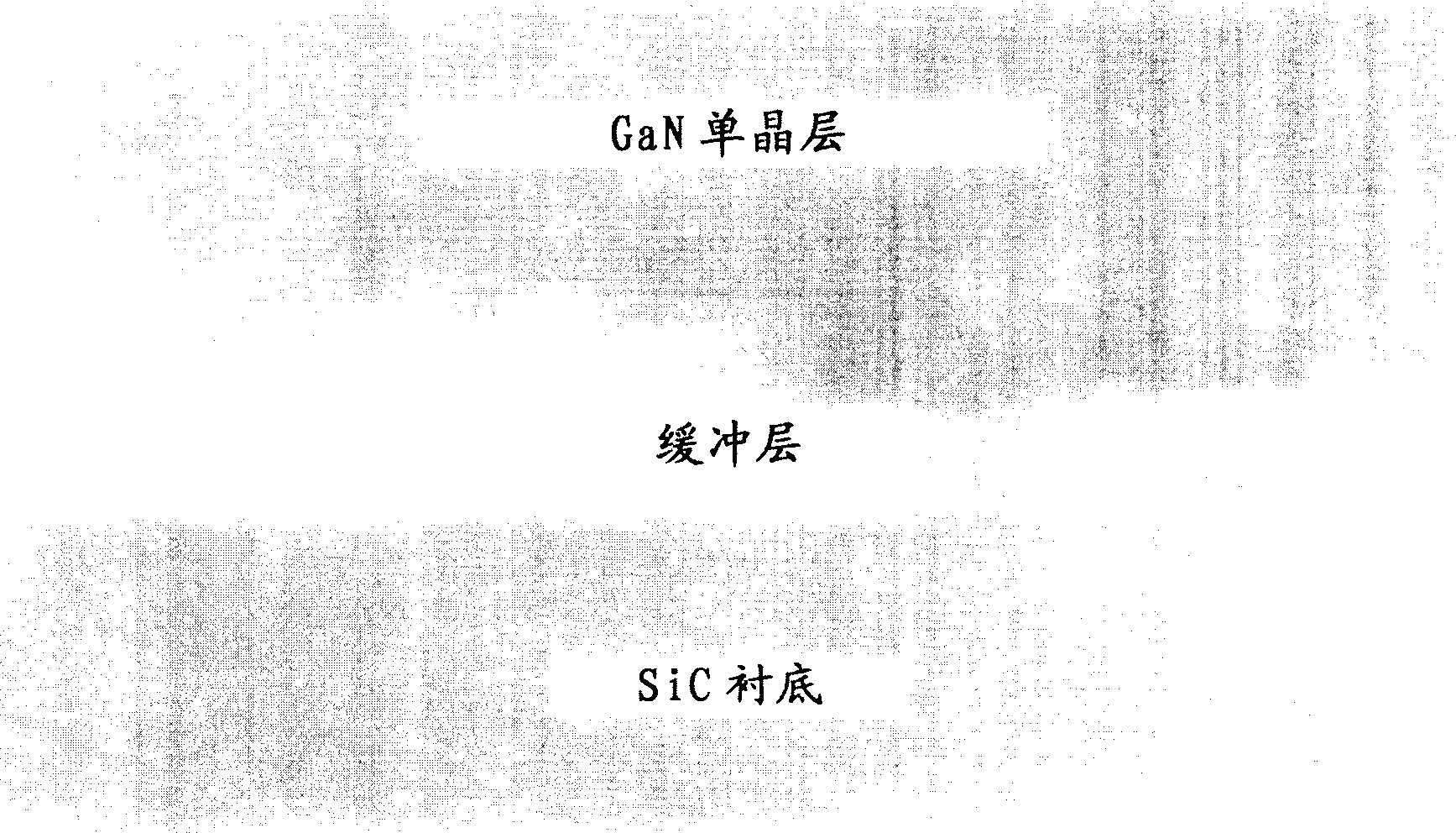
Group ó¾ nitride semiconductor multilayer structure
A technology of nitride semiconductor and multi-layer structure, which is applied in the direction of semiconductor devices, semiconductor/solid-state device manufacturing, electrical components, etc., and can solve problems such as increasing manufacturing costs and complex processes
- Summary
- Abstract
- Description
- Claims
- Application Information
AI Technical Summary
Problems solved by technology
Method used
Image

Examples
example 1
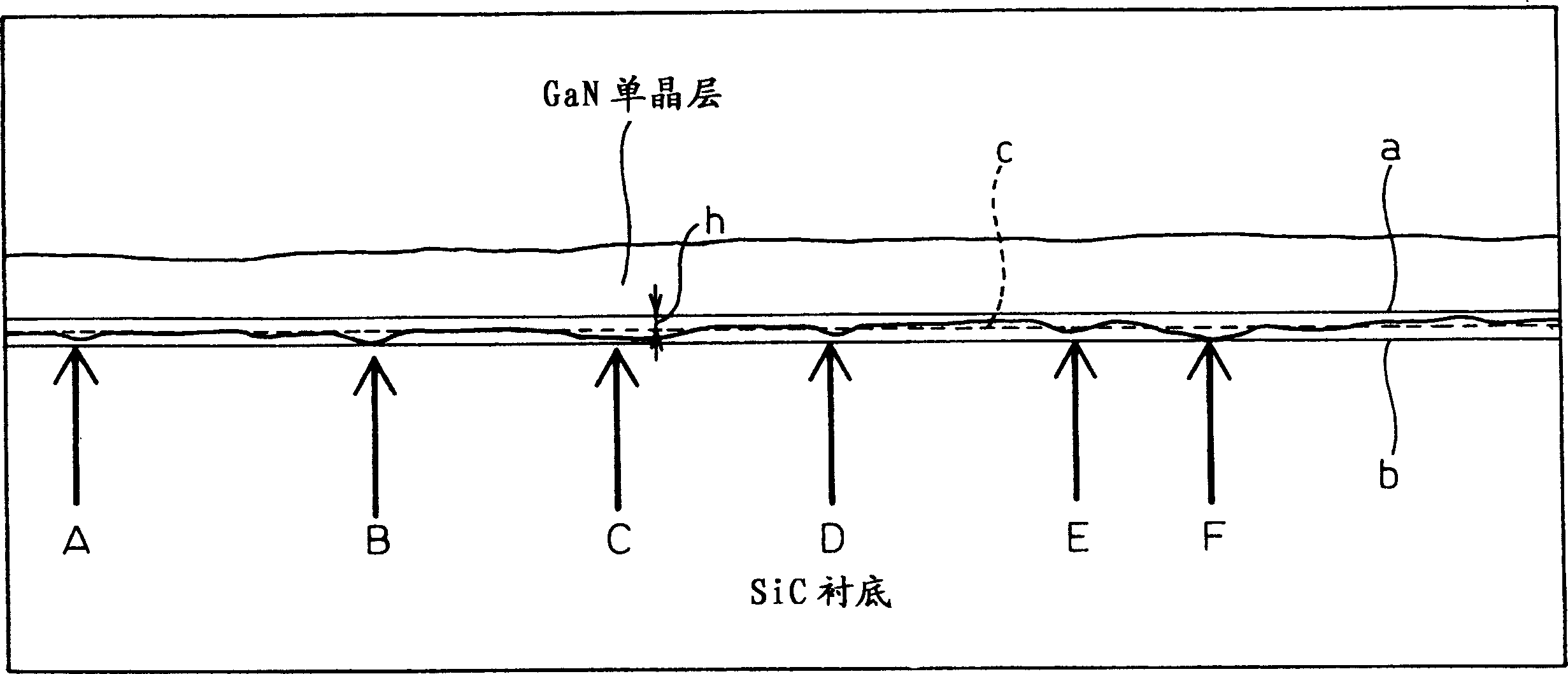
[0066] Sheet SiC single crystal substrates with a thickness of 450 μm were cut from n-SiC ingots by batch slicing method using #400 electrodeposition wire saw. During the slicing process, non-periodically distributed grooves (scratches) are formed on the cut surface of the substrate (density: several to 10 grooves / 0.1 mm). The depth of the deepest grooves was found to be about 1 μm; ie the average depth of the grooves was found to be about 0.5 μm.
[0067] After rinsing the substrate with acetone, the substrate was subjected to a surface etching treatment by using a dry etching device to remove the process-affecting layer from the substrate. Specifically, the substrate was subjected to an etching process for five minutes by using a gas containing chlorine under the following conditions: RF power: 1 kW, bias power: 300 W. The average etching depth was adjusted to 2 μm. Even after the etching process, it was observed that the aperiodic distribution of trenches remained on the ...
example 2
[0075] The procedure of Example 1 was repeated except that the growth temperature of the GaN single crystal layer was adjusted to 1,000° C., thereby manufacturing a Group III nitride semiconductor multilayer structure. The semiconductor multilayer structure thus obtained exhibits satisfactory smoothness, although a small amount of pits remain on the surface of the multilayer structure, and it is found that the surface roughness (Ra) of the multilayer structure is 100 nm, which is the same as that of Example 1. This value is higher than in the case of a semiconductor multilayer structure.
example 3
[0077] By utilizing the group III nitride semiconductor multilayer structure of Example 1, a GaN type light emitting device with an emission wavelength of 460 nm was manufactured by a method known in the art.
[0078] Specifically, after growing the GaN single crystal layer in Example 1, by using SiH as a dopant 4 An n-type layer (carrier concentration: 1×10 19 / cm 3 ). Thereafter, the substrate temperature was lowered to 750 °C, and the MQW light-emitting layer formed of five layer units each including In 0.16 Ga 0.84 N layer (thickness: 3nm) and GaN layer (thickness: 7nm). Subsequently, the substrate temperature was raised again, and a p-type layer (thickness: 100nm) formed of a magnesium-doped GaN layer was laminated
[0079] Subsequently, through typical photolithography and dry etching techniques, part of the p-type layer and part of the light emitting layer are removed, so that the n-type layer doped with silicon is exposed to the outside. Thereafter, a Ti / Al negat...
PUM
| Property | Measurement | Unit |
|---|---|---|
| thickness | aaaaa | aaaaa |
| thickness | aaaaa | aaaaa |
| depth | aaaaa | aaaaa |
Abstract
Description
Claims
Application Information