Method for preparing full solid electrochromic device with sol-gel
An electrochromic device and electrochromic layer technology, applied in the field of functional devices and electrochemical materials, can solve the problems of high manufacturing cost, complicated process control, etc., and achieve the effects of low cost, simple process equipment, and easy application and promotion
- Summary
- Abstract
- Description
- Claims
- Application Information
AI Technical Summary
Problems solved by technology
Method used
Image
Examples
Embodiment 1
[0038] Preparation of electrochromic device preparation layer:
[0039] (1) Preparation of transparent conductive layer:
[0040] The raw materials used are as follows:
[0041] Nano Indium Tin Oxide Ethanol Paste (20-30nm) Ningxia Dongfang Nonferrous Metals Group
[0042] Butanol (analytical grade AR) Shanghai Lingfeng Chemical Reagent Co., Ltd.
[0043] Hydrochloric acid (analytical pure AR) Sinopharm Chemical Reagent Co., Ltd.
[0044] Silane coupling agent (KH560) Nanjing Hefu Chemical Factory
[0045]Silica Sol (FSI) Zhejiang Yuda Chemical Co., Ltd.
[0046] Ethanol (analytical grade AR) Sinopharm Chemical Reagent Co., Ltd.
[0047] Ethyl Orthosilicate Shanghai Chemical Reagent Purchasing Supply Wulian Chemical Factory
[0048] Epoxy Resin (E-51) Zhejiang Jiahua Industrial Co., Ltd.
[0049] Maleic acid (analytical pure AR) Sinopharm Chemical Reagent Co., Ltd.
[0050] The raw material ratio of the self-made film-forming agent is as follows:
[0051] 25 parts (we...
Embodiment 2
[0085] Preparation of transparent conductive layer:
[0086] The raw materials used are as follows:
[0087] Aluminum-doped zinc oxide (AZO) (20-30nm) Ningxia Dongfang Nonferrous Metals Group.
[0088] The raw material ratio of the prepared transparent conductive layer is as follows:
[0089] AZO homogeneously dispersed slurry 100 parts (weight)
[0090] 15 parts (weight) of film-forming agent
[0091] 10 parts of hydrochloric acid (weight)
[0092] 2 parts of n-butanol (by weight)
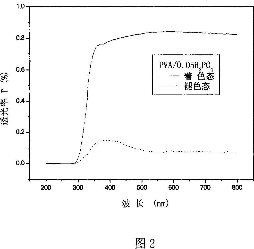
[0093] The preparation of the film-forming agent, the preparation process of the transparent conductive layer and the preparation process of other layers and device assembly of the all-solid-state electrochromic device are similar to those shown in Example 1, and the electrochromic performance of the obtained device is similar to that shown in FIG. 2 .
Embodiment 3
[0095] Preparation of transparent conductive layer:
[0096] The raw materials used are as follows:
[0097] Aluminum-doped zinc oxide (AZO) (20-30nm) Ningxia Dongfang Nonferrous Metals Group.
[0098] The raw material ratio of the prepared transparent conductive layer is as follows:
[0099] AZO homogeneously dispersed slurry 100 parts (weight)
[0100] 15 parts (weight) of film-forming agent
[0101] 10 parts of hydrochloric acid (weight)
[0102] 2 parts of n-butanol (by weight)
[0103] The preparation of the film-forming agent, the preparation process of the transparent conductive layer and the preparation process of other layers and device assembly of the all-solid-state electrochromic device are similar to those shown in Example 1, and the electrochromic performance of the obtained device is similar to that shown in FIG. 2 .
PUM
 Abstract
Description
Claims
Application Information

