

InGaN series broad band solar battery comprising multiple quanta structure
A multi-quantum well structure and solar cell technology, which is applied in the field of InGaN-based broad-spectrum solar cells, can solve problems such as reducing battery performance, and achieve the effects of improving performance, realizing energy conversion efficiency, and reducing dark current.
- Summary
- Abstract
- Description
- Claims
- Application Information
AI Technical Summary
Problems solved by technology
Method used
Image

Examples
Embodiment 1
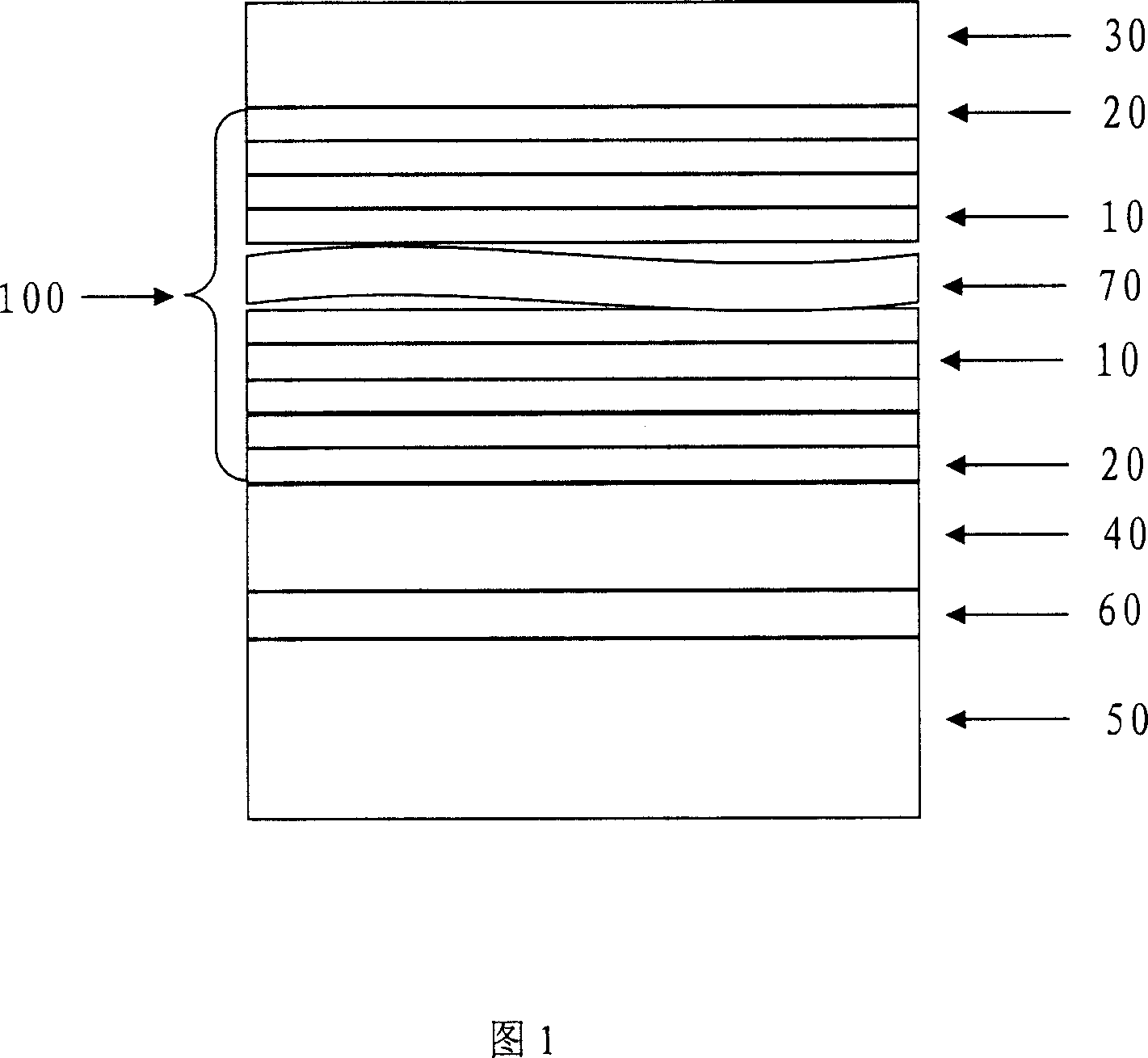
[0025] As shown in FIG. 1 , on a sapphire substrate, MOCVD epitaxial growth technology is used to epitaxially grow the InGaN system wide-spectrum single-junction solar cell structure containing multiple quantum wells of the present invention. First, a 1 micron GaN transition layer 60 is grown on the substrate 50, followed by a 500 nm p-type In 0.4 Ga 0.6 N (the doped impurity is Mg, the doping concentration is 5×10 17 cm -3 ) layer 40, 30 cycles of In 0.45 Ga 0.55 N (quantum well width 4nm) / In 0.4 Ga 0.6 N (barrier width 10nm) (10 / 20), then 300nm n-type In 0.4 Ga 0.6 N (the doped impurity is Si, the doping concentration is 1×10 18 cm -3 ) layer 30 to obtain the InGaN-based single-junction solar cell structure containing multiple quantum wells of the present invention. The photoelectric conversion efficiency of this structure is greater than 20%.
Embodiment 2
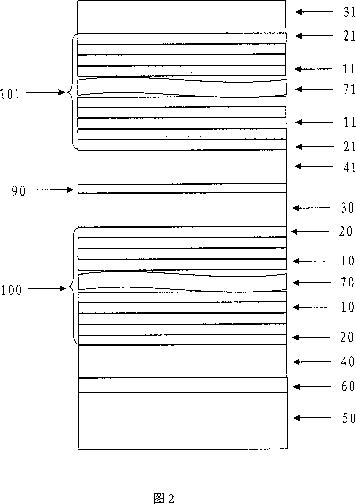
[0027] As shown in FIG. 2 , on a sapphire substrate, MOCVD epitaxial growth technology is used to epitaxially grow the InGaN system wide-spectrum two-junction solar cell containing the multi-quantum well structure of the present invention. First, a 1 micron transition layer 60 of GaN and InGaN combination is grown on the substrate 50; then a bottom junction cell with a narrow bandgap is grown, and the structure of this cell is: 500nm p-type In 0.55 Ga 0.45 N (the doped impurity is Zn, the doping concentration is 3×10 17 cm -3 ) layer 40, 20 cycles of In 0.6 Ga 0.4 N (quantum well width 3nm) / In 0.65 Ga 0.45 N (barrier width 8nm) (10 / 20), then 200nm of n-type In 0.55 Ga 0.45 N (doped impurity is Si, doping concentration 2×10 18 cm -3 ) layer 30; a tunnel junction 90 connected to the top junction is grown thereon; a top junction cell structure is grown on the tunnel junction 90, and the structure of each layer of the top junction cell is: 400nm p-type In 0.4 Ga 0.6 N (...
Embodiment 3
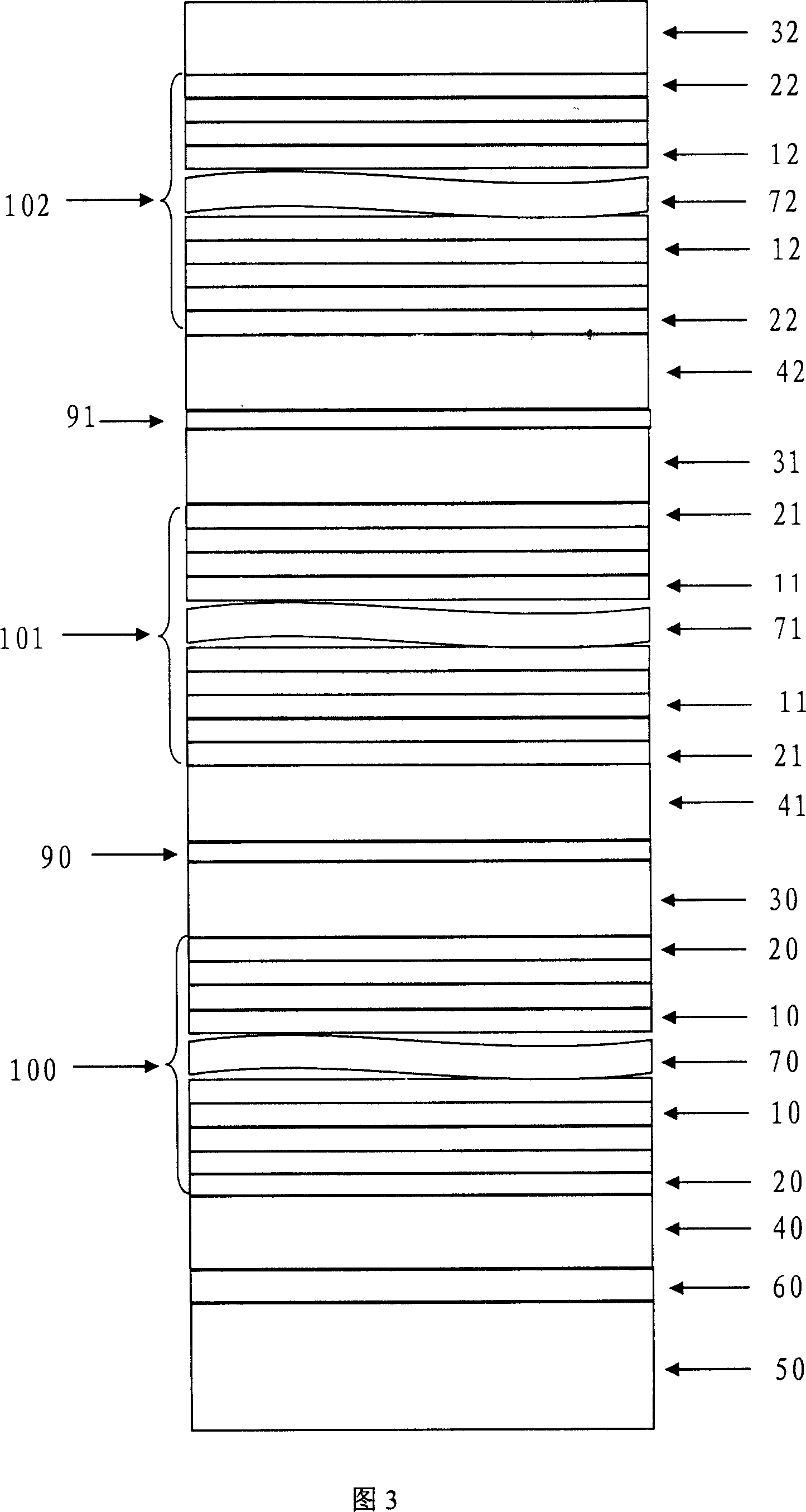
[0029] On the Si substrate, the InGaN wide-spectrum two-junction solar cell structure containing multiple quantum wells of the present invention is epitaxially grown by using MOCVD epitaxial growth technology. First, grow an 800nm AlGaN transition layer on the Si substrate; then grow a bottom junction cell with a narrow band gap, the structure of this cell is: 500nm p-type In 0.55 Ga 0.45 N (the doped impurity is Mg, the doping concentration is 3×10 17 cm -3 ) layer, 35 cycles of In 0.6 Ga 0.4 N (quantum well width 3nm) / In 0.55 Ga 0.45 N (barrier width 8nm), then 200nm of n-type In 0.55 Ga 0.45 N (the doped impurity is Si, the doping concentration is 3×10 18 cm -3 ) layer; a tunnel junction connected to the top junction is grown on it; a top junction cell structure is grown on the tunnel junction, and the structure of each layer of the top junction cell is: 800nm p-type In 0.4 Ga 0.6 N (doped impurity is Mg, doping concentration 2×10 17 cm -3 ) layer and 600nm...
PUM
| Property | Measurement | Unit |
|---|---|---|
| Thickness | aaaaa | aaaaa |
| Thickness | aaaaa | aaaaa |
| Thickness | aaaaa | aaaaa |
Abstract
Description
Claims
Application Information