Semiconductor laser element

一种激光元件、半导体的技术,应用在半导体激光器、激光器零部件、激光器等方向,能够解决斜率效率低、寿命降低、端面老化等问题,达到抑制老化、高输出的效果

Active Publication Date: 2007-03-14
NICHIA CORP
View PDF2 Cites 8 Cited by
  • Summary
  • Abstract
  • Description
  • Claims
  • Application Information

AI Technical Summary

Problems solved by technology

[0007] However, when Al with a thickness of λ / 2n 2 o 3 When the film is formed by a single layer, the amorphous Al 2 o 3 When the film is driven with a high output of 30mW or more, it reacts as a semiconductor element, causing aging of the end face
In addition, for single crystal Al 2 o 3 The stress of the film is large, so there is heat generated during driving, and the Al 2 o 3 Problems such as film and semiconductor element peeling
[0008] In addition, when a semiconductor laser element using a nitride semiconductor is operated at a high output, for example, 30 mW or more, when a dielectric film is formed as a single film on the end surface on the light-emitting side, damage to the end surface is likely to occur. , so that there is a problem of reduced lifespan
In addition, when operating at high output, if the slope efficiency is low, there will be a problem that the drive current will increase.

Method used


Image

  • Semiconductor laser element
  • Semiconductor laser element
  • Semiconductor laser element

Examples


Embodiment 1

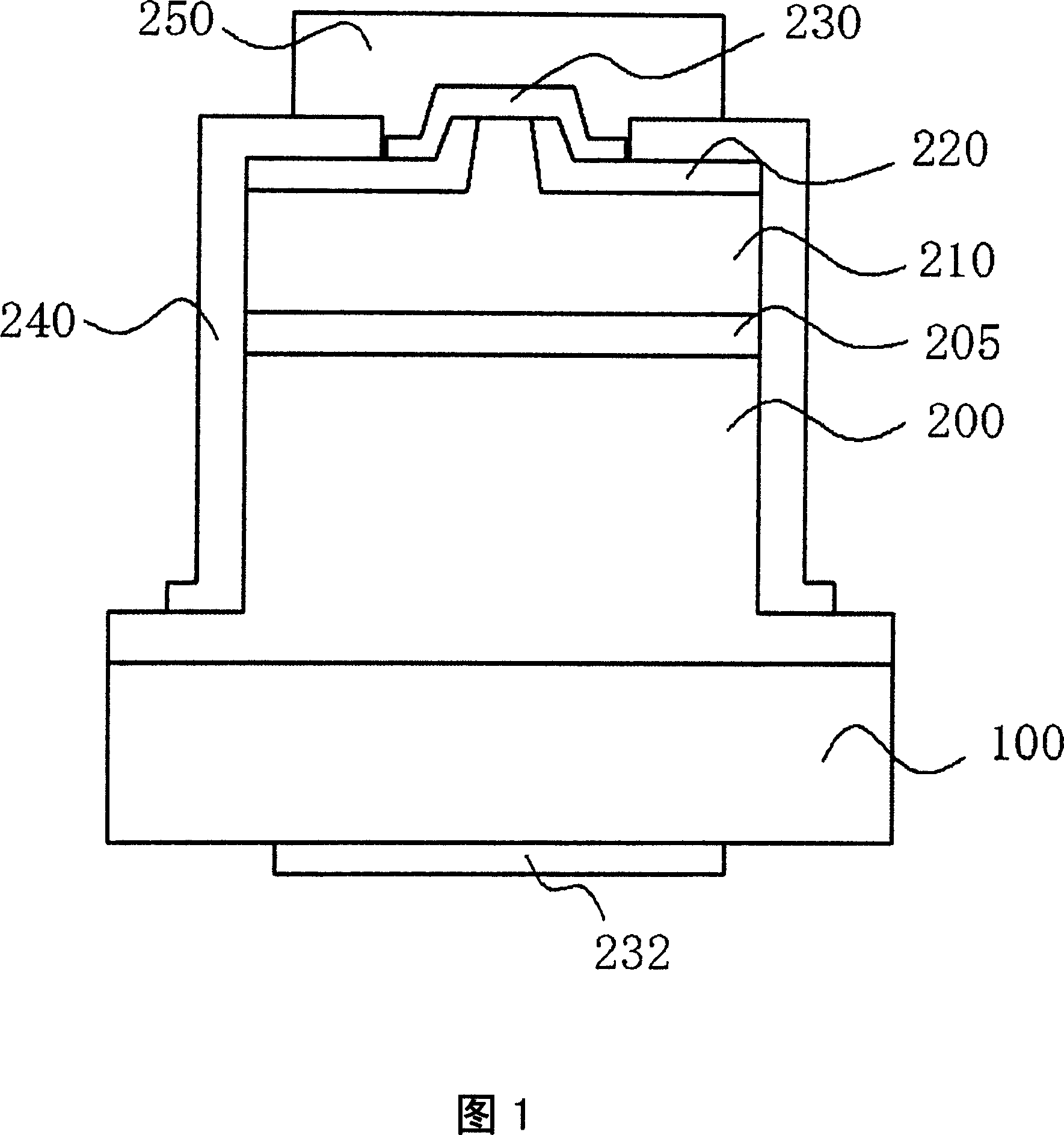
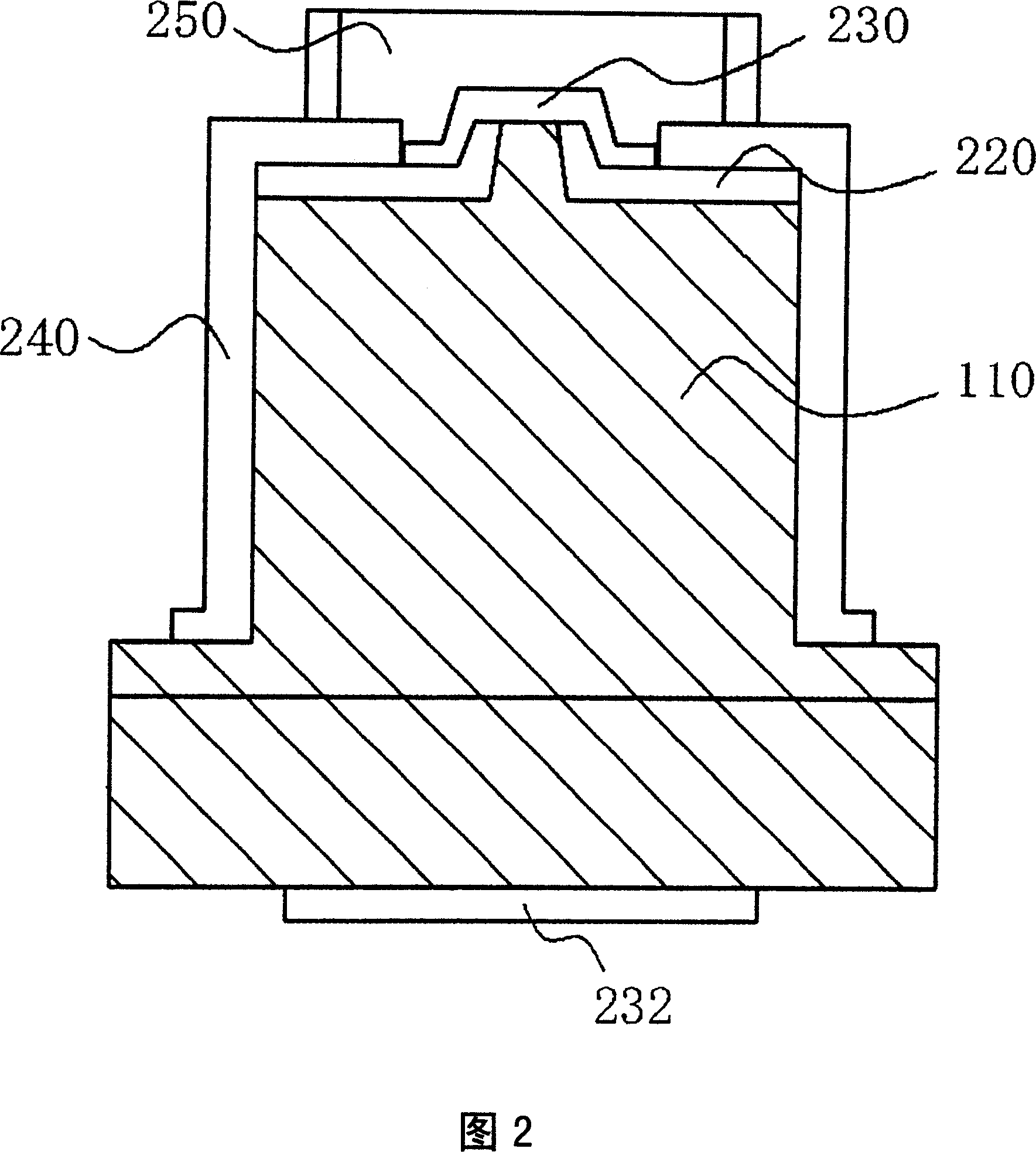
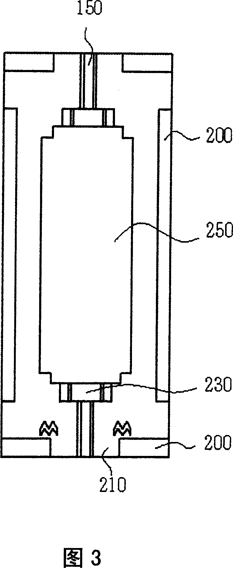
[0098] As the substrate, a wafer-like GaN substrate 100 having a C plane as a main surface was used. The substrate is not particularly limited thereto, and a GaN substrate whose main surfaces are the R plane and the A plane can be used as needed.

[0099] (n-type cladding layer 201) Next, the GaN substrate was transferred to an MOCVD apparatus. The atmosphere temperature in the furnace was set at 1050°C, and TMA (trimethylaluminum), TMG, and ammonia were used as raw material gases to grow undoped Al 0.04 Ga 0.96 An n-type cladding layer composed of N. This layer may also be doped with n-type impurities.

[0100] (Active layer 205) Next, set the temperature to 800°C, use TMI (trimethylindium), TMG, and ammonia as raw materials, and use silane gas as an impurity gas to grow Si-doped In with a film thickness of 140 Å. 0.02 Ga 0.98 The barrier layer composed of N. Next, the use of silane gas was stopped, and undoped In was grown with a film thickness of 80 Ȧ 0.1 Ga 0.9 Wel...

Embodiment 2

[0118] A nitride semiconductor laser element was formed in the same manner as in Example 1, except that the dielectric film 110 on the light-exit side end face had the following configuration. An ECR sputtering device was used. After cleaning the light exit side end face with plasma of active gas such as oxygen, the x o y The first dielectric film and the second dielectric film are formed. First, use 5N Al in the metal target, set the flow rate of Ar to 15 sccm; 2 The flow rate was set to 10 sccm; the microwave power was 600 W; and the RF was 600 W, the first dielectric film was formed with a film thickness of 20 nm. Thereafter, using 5N Al in the metal target, the flow rate of Ar is set to 10 sccm; the O 2 The flow rate was set at 3 sccm, the microwave power was 450 W, and the RF was 450 W, and the second dielectric film was formed with a film thickness of 100 nm. Here, with respect to light of 405 nm, the refractive index of the first dielectric film is 1.63, and the re...

Embodiment 3

[0120] A nitride semiconductor laser device was formed in the same manner as in Example 1, except that the dielectric film had the following configuration.

[0121] For the end face on the light exit side, after using an ECR sputtering device to clean the end face on the light exit side with plasma of an active gas such as oxygen, use 5N Al in the metal target, and set the flow rate of Ar to 15 sccm; 2 The flow rate is set to 10sccm; the microwave power is 600W; RF is 600W, after the first dielectric film 111 is formed with a film thickness of 20nm, 5N Al is used in the metal target, and the flow rate of Ar is set to 10sccm; Will O 2 The flow rate was set at 3 sccm; the microwave power was 450 W; and the RF was 450 W, the second dielectric film was formed with a film thickness of 40 nm, thereby forming the dielectric film 110 . Here, with respect to light of 405 nm, the refractive index of the first dielectric film is 1.63, and the refractive index of the second dielectric fi...


PUM


Abstract

A semiconductor laser device, which has a protective film at an end surface thereof, is adaptable to demands for higher outputs or shorter wavelengths. The semiconductor laser device according to the present invention includes a dielectric film on at least one end surface of an optical resonator, in which the dielectric film includes a first dielectric layer and a second dielectric layer comprised of the same elements and disposed in sequence from the end surface side of the semiconductor, the first dielectric layer including a layer made of a single crystal material and the second dielectric layer including a layer made of an amorphous material.

Description

technical field [0001] The invention relates to a semiconductor laser element, in particular to a high-output semiconductor laser element with an oscillation wavelength below 600nm. Background technique [0002] Currently, high-output semiconductor laser elements are required for writing applications in optical disks or magneto-optical disks. These semiconductor laser elements are required to operate stably in the fundamental mode for a long time. [0003] In addition, in order to realize the shortening of the wavelength required for the high density of optical discs, semiconductor laser elements using nitride semiconductors are being studied. Semiconductor laser devices using nitrides can be used in light sources for exposure, light sources for printing machines, light sources for medical treatment, light sources for optical communication systems, measurements, etc., in addition to light sources for optical discs. In addition, since laser elements made of nitride semicond...

Claims


Application Information

Patent Timeline
Patent Type & Authority Applications(China)
IPC IPC(8): H01S5/00H01S5/10
CPCH01S5/0287H01S5/34333H01S5/028H01S5/16H01S5/0282B82Y20/00H01S5/30
Inventor 落合真尚汤浅功治
Owner NICHIA CORP
Why Eureka
Try Eureka