Composition for charge transport membrane and ionic compound, charge transport membrane and organic electroluminescent device each using the same, and method for producing the device and membrane
A technology for charge transport membranes and ionic compounds, which is applied in the field of charge transport membrane compositions and ionic compounds, and can solve the serious problems of display performance stability of display devices, etc.
- Summary
- Abstract
- Description
- Claims
- Application Information
AI Technical Summary
Problems solved by technology
Method used
Image
Examples
Embodiment 1
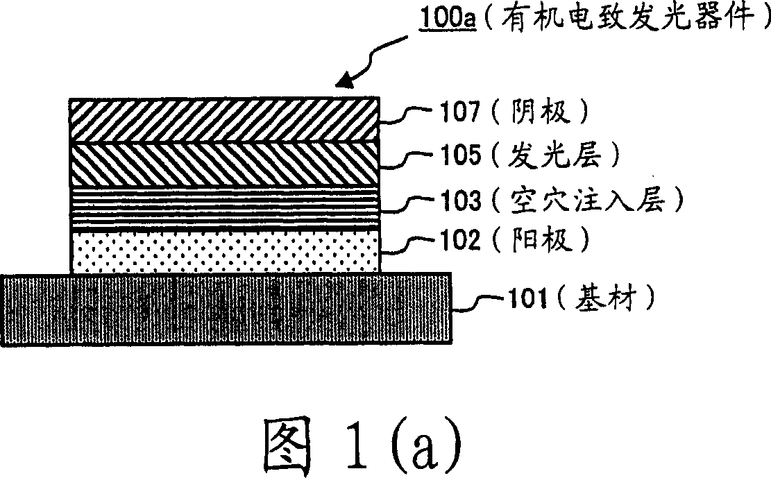
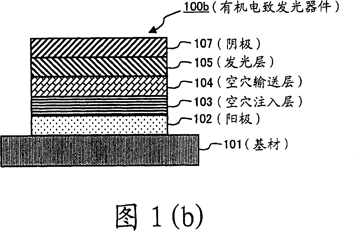
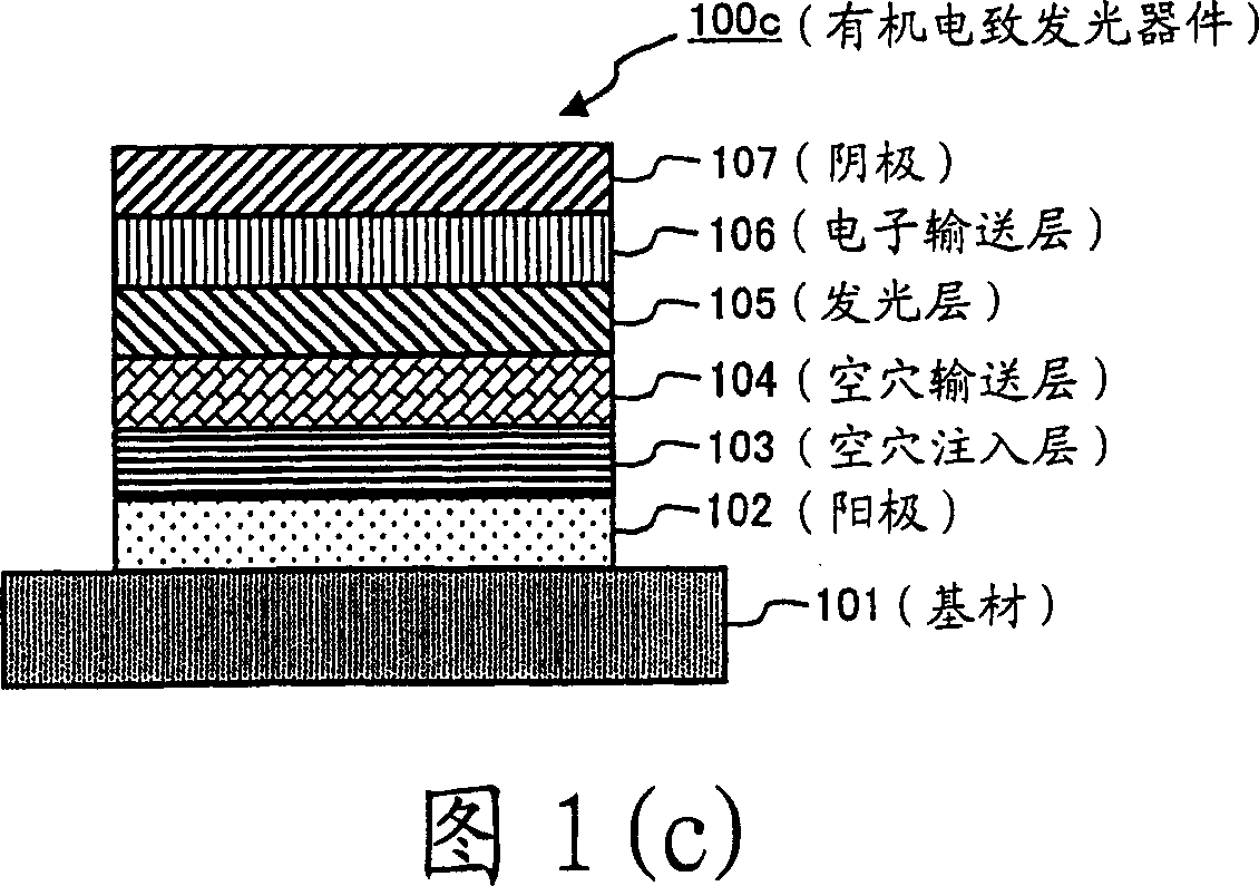
[0401] An organic electroluminescent device having a layer constitution similar to that of the organic electroluminescent device 100b shown in FIG. 1(b) was produced by the following method.
[0402] A 120nm-thick indium tin oxide (ITO) transparent conductive film was deposited on a glass substrate (sputtered film product manufactured by Sanrong Vacuum Co., Ltd.) using conventional photolithography technology and hydrogen chloride etching, thereby forming a width of 2mm. strip pattern to prepare the anode. The patterned ITO substrate was sequentially subjected to ultrasonic cleaning in aqueous surfactant solution, ultrapure water washing, ultrasonic cleaning in ultrapure water, and ultrapure water washing, followed by drying with compressed air, and finally ultraviolet ray cleaning. -Ozone cleans.
[0403] The following composition was spin-coated on the above-mentioned glass substrate under the conditions shown in Table 12 below to form a uniform film with a thickness of 30 ...
Embodiment 2
[0416] Except adding 0.2% by weight of the compound (B-30) shown in the above table as the ionic compound instead of the ionic compound (A-1), the same procedure as in Example 1 was performed, thereby preparing an organic electroluminescent device . The light emitting characteristics of the obtained devices are shown in Table 15. A device capable of emitting light at low voltage even at a heat-drying temperature of 200°C was obtained.
Embodiment 3
[0429] Except for preparing a hole injection layer under the conditions shown below, the same procedure as in Example 1 was performed to obtain an organic electroluminescent device.
[0430] solvent
[0431] The light emitting characteristics of the obtained devices are shown in Table 20. As shown in Table 20, under the drying conditions of 230° C. and 15 minutes of heating, devices emitting light at low voltage were obtained.
PUM
| Property | Measurement | Unit |
|---|---|---|
| thickness | aaaaa | aaaaa |
| thickness | aaaaa | aaaaa |
| thickness | aaaaa | aaaaa |
Abstract
Description
Claims
Application Information


