Quantum trap structure of semiconductor light-emitting diode for increasing internal quantum efficiency

A light-emitting diode and internal quantum efficiency technology, applied in the field of quantum well structures, can solve the problems of reducing the probability of radiation recombination, reducing the probability of tunneling, and reducing the quality of the crystal of the quantum well layer.

Active Publication Date: 2007-03-28
HC SEMITEK SUZHOU
View PDF0 Cites 12 Cited by
  • Summary
  • Abstract
  • Description
  • Claims
  • Application Information

AI Technical Summary

Problems solved by technology

It has two disadvantages. First, this layer only has a significant effect on the adjacent quantum wells. For multiple quantum well structures, due to the thick barrier, the tunneling probability is reduced, and the latter quantum wells will not be significantly affected by the existence of this layer. Increase the probability of electron capture; second, the existence of this layer may lead to a decrease in the quality of the quantum well layer crystal, resulting in V-type defects, increasing leakage current, and reducing the probability of radiation recombination

Method used


Image

  • Quantum trap structure of semiconductor light-emitting diode for increasing internal quantum efficiency
  • Quantum trap structure of semiconductor light-emitting diode for increasing internal quantum efficiency
  • Quantum trap structure of semiconductor light-emitting diode for increasing internal quantum efficiency

Examples


Embodiment Construction

[0033] specific implementation

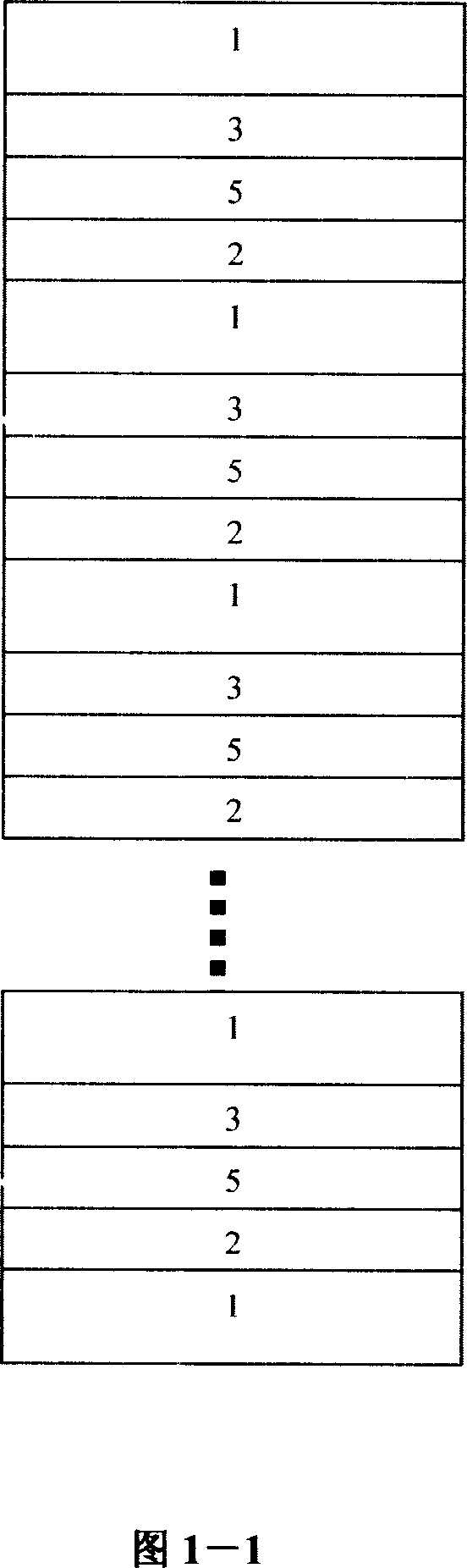
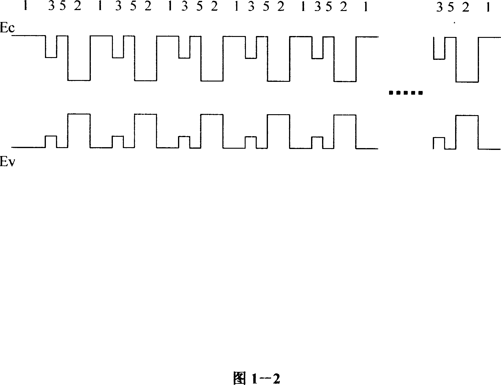
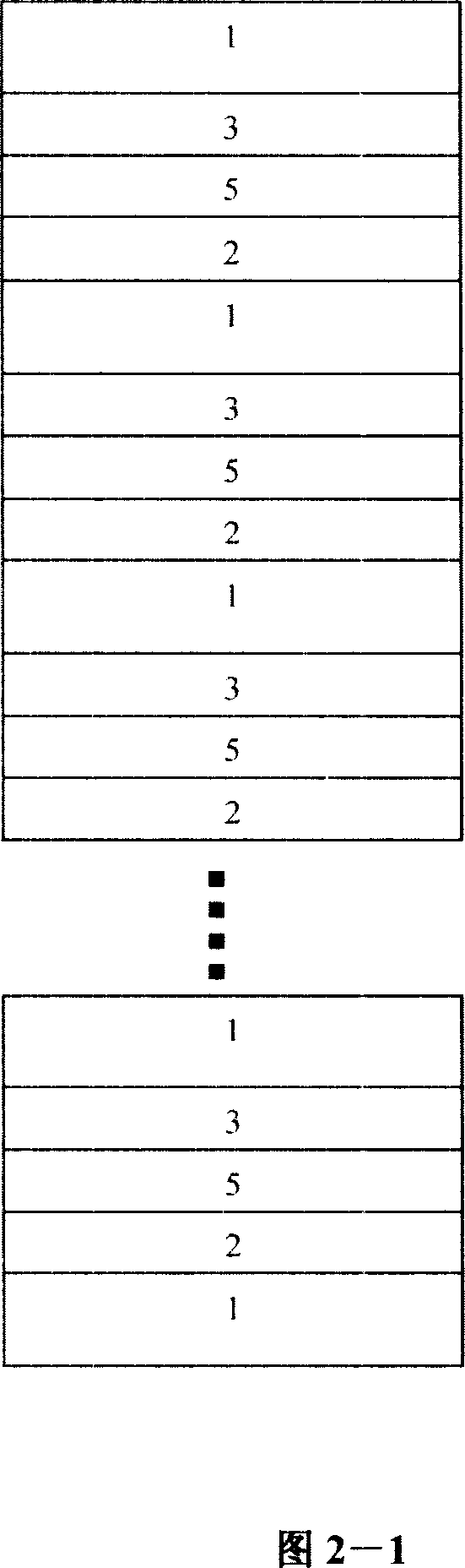
[0034] Embodiments 1-4 of the novel quantum well structure of the present invention can be seen in Fig. 1-1 to Fig. 4-1.

[0035] Figure 1-1 is a quantum well structure with increased electron capture capability for blue light-emitting diodes, and a schematic diagram of energy bands 1-2; wherein, viewed from top to bottom, layers 1, 3, 5 and 2 form a period and repeat , the number of cycles can be selected from 1 to 10. Layer 1 is a barrier layer made of gallium nitride with a thickness between 5nm and 20nm. Layer 2 is a quantum well layer, composed of indium gallium nitride alloy, with a thickness between 1nm and 5nm, an indium composition between 15% and 25%, and a corresponding emission wavelength between 450nm and 500nm. Layer 3 is an in-situ electron capture emission layer, which is composed of indium gallium nitride alloy, with a thickness between 1nm and 3nm and an indium composition between 3% and 10%. Layer 5 is a tunneling barrier ...


PUM


Abstract

Characters of the disclosed structure of quanta trap are that through tunneling barrier layer 5 with high tunneling probability, home position electron capture layer 3 or home position hole capture layer 4 are connected to quanta trap layer 2; layres 1, 3 or 4, 5 and 2 constitute a cycle to carry out activity repeatedly. Number of cycles can be selected from 1 to 10; both of upmost and undermost layers are barrier layers 1; thickness of home position electron capture layer 3 or home position hole capture layer 4 is between 1nm to 3nm. Being as active layer, the structure can increase probability of capturing electrons or holes so as to raise internal quantum efficiency of gallium nitride based light emitting diode of blue green light.

Description

technical field [0001] The invention relates to a novel quantum well structure that can be applied to semiconductor light-emitting diodes, especially gallium nitride-based blue-green light-emitting diodes, and can effectively increase the internal quantum efficiency, and can be used as an active material for gallium nitride-based blue-green light-emitting diodes. Area. Background technique [0002] Semiconductor light-emitting diodes have the advantages of high luminous efficiency, long life, small size, and rich colors, and have been widely valued. They are currently used in many fields, including traffic lights, mobile phone display backlights, button backlights, and indoor and outdoor full-color displays. , landscape lighting, special lighting, etc. With the further improvement of device performance, semiconductor light-emitting diodes will gradually penetrate into larger markets such as LCD TV backlights, LCD computer display backlights, and general lighting. [0003] ...

Claims


Application Information

Patent Timeline
Patent Type & Authority Applications(China)
IPC IPC(8): H01L33/00H01S5/343H01L33/06
Inventor 刘伟
Owner HC SEMITEK SUZHOU
Why Eureka
Try Eureka