

An organic light-emitting display device electrode substrate
A technology for light-emitting display devices and electrode substrates, which is applied to electric solid-state devices, semiconductor devices, semiconductor/solid-state device components, etc., can solve the problems of difficult etching process, prolonged substrate etching cycle, etc., and achieves improved display efficiency, reduced resistance, Deterioration prevention effect
- Summary
- Abstract
- Description
- Claims
- Application Information
AI Technical Summary
Problems solved by technology
Method used
Image

Examples
Embodiment 1
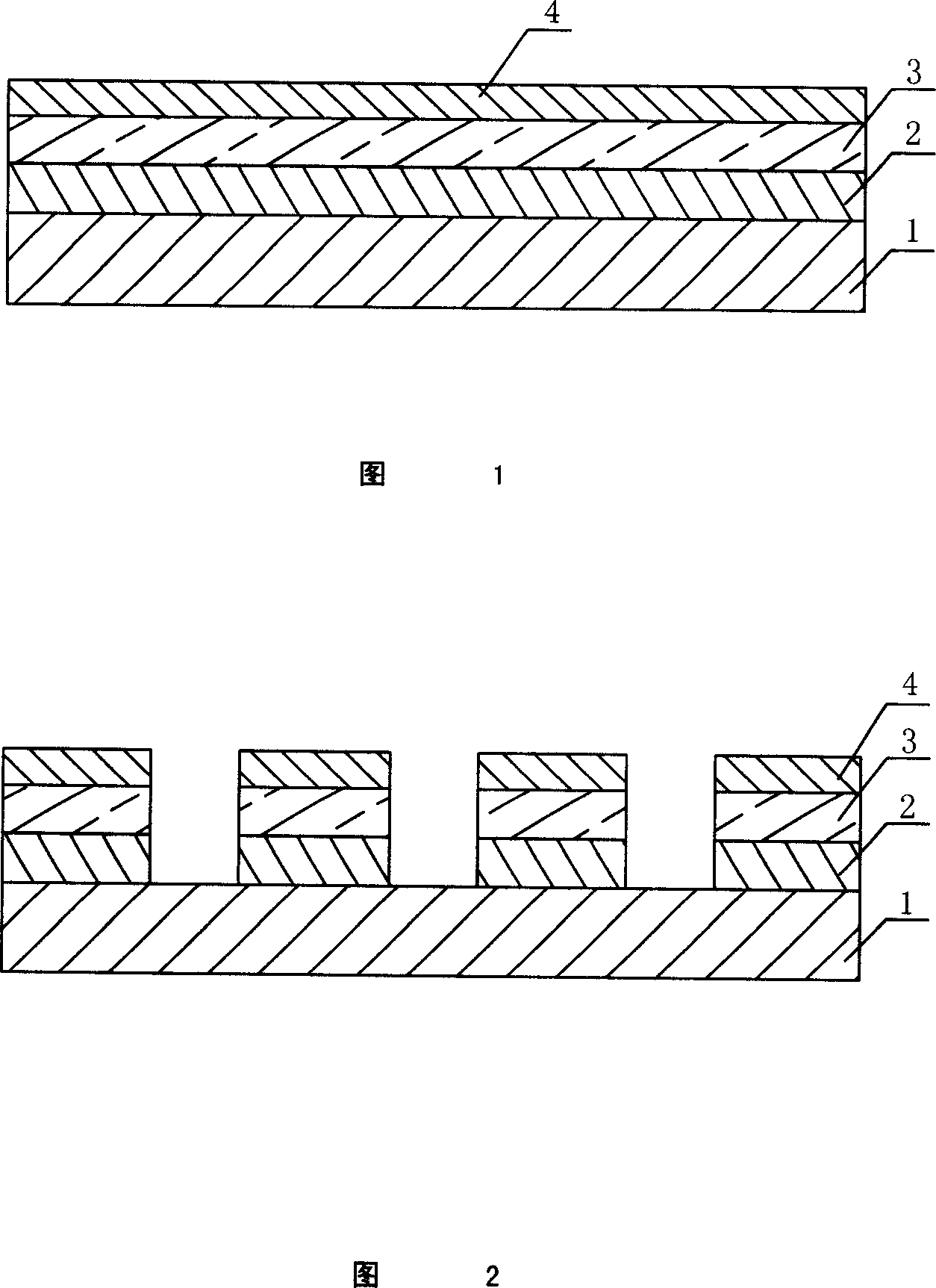
[0021] Refer to Figures 1 and 2. The organic light-emitting display device electrode substrate of this embodiment includes ITO (150nm) serving as the electrode layer 1, and silver metal (160nm) serving as the wire layer 2, on which a vanadium metal protective layer 3 is prepared by sputtering, with a thickness of 15nm.
[0022] The metal silver wire layer 2 and the metal vanadium protective layer 3 are simultaneously etched with an etching solution with a volume ratio of phosphoric acid: nitric acid: water = 9:1:3, and the etching rate is 40A / s. The underlying ITO is etched with an etching solution with a volume ratio of nitric acid:hydrochloric acid:water=1:10:10, and the etching rate is 10A / s. Through the above conditions, the structure shown in Figure 2 can be prepared. The surface resistance of the wire layer 2 is 0.1 ohm / sq, and when heated at 120° C. for 30 minutes, the surface resistance is 0.11 ohm / sq, showing good stability.
Embodiment 2
[0024] Refer to Figures 1 and 2. The organic light emitting display device electrode substrate of this embodiment includes ITO (150 nm) used as the electrode layer 1 and aluminum metal (300 nm) used as the wiring layer 2 . On it, the method of dual-source evaporation is adopted, and the mixture of metal indium and metal palladium is evaporated as the protective layer 3, and the evaporation mass ratio of metal indium and metal palladium is controlled to be a metal mixed layer of 9.5:1, that is, the metal mixed layer of the protective layer 3 The thickness is 15nm.
[0025] The wire layer 2 of metal aluminum and the protective layer 3 of a mixture of metal indium and metal palladium are simultaneously etched with an etching solution with a volume ratio of phosphoric acid: nitric acid: water = 8:1:3, and the etching rate is 30A / s. The underlying ITO is etched with an etching solution with a volume ratio of nitric acid:hydrochloric acid:water=1:10:10, and the etching rate is 10A / ...
Embodiment 3
[0027] Refer to Figures 1 and 2. The organic light-emitting display device electrode substrate of this embodiment includes ITO (150nm) used as the electrode layer 1, and copper-silver alloy (300nm) used as the wire layer 2. The composition of the copper-silver alloy is copper:silver=1:9. A sputtering method is adopted on it, and zinc oxide is sputtered as the protective layer 3, and the thickness of the protective layer 3 is 12nm.
[0028] The copper-silver alloy wire layer 2 and the zinc oxide protective layer 3 are simultaneously etched with an etching solution with a volume ratio of phosphoric acid: nitric acid: water = 9:2:3, and the etching rate is 60A / s. The underlying ITO is etched with an etching solution with a volume ratio of nitric acid:hydrochloric acid:water=1:10:10, and the etching rate is 10A / s. Through the above conditions, the structure shown in Figure 2 can be prepared. The surface resistance of the wire layer 2 is 0.25 ohm / sq, and when heated at 120° C. fo...
PUM
| Property | Measurement | Unit |
|---|---|---|
| Thickness | aaaaa | aaaaa |
| Thickness | aaaaa | aaaaa |
| Surface resistance | aaaaa | aaaaa |
Abstract
Description
Claims
Application Information