Scintillation detector for detection of ionising radiation

a technology of ionising radiation and detector, which is applied in the direction of instruments, particle separator tube details, x/gamma/cosmic radiation measurement, etc., can solve the problem of not considering the strong piezoelectric field, the ratio of consumed energy for radiative and non-radiative recombination still cannot suffice, and the effect of high luminescence intensity and short decay tim

Active Publication Date: 2018-09-04
CRYTUR SPOL SRO +1
View PDF1 Cites 0 Cited by
  • Summary
  • Abstract
  • Description
  • Claims
  • Application Information

AI Technical Summary

Benefits of technology

[0010]The advantages of the scintillation detector with principally the same polarisation of active couple layers include a short decay time which is in units of nanoseconds and high luminescence intensity, caused by improved overlap of the hole and electron wave functions. Another manner of increasing the overlap of the electron and hole wave functions is the insertion of the carrier attracting layer that pulls inside itself electrons and holes which results in electron and hole spatial approximation, thus increasing the excited luminescence intensity and making faster the scintillator luminesce response.
[0011]In another preferred execution of the scintillation detector with GaN buffer layer according to this invention, the composition and thickness of the barrier layer and the layer representing the potential well conform to the relation|d1·(4.3·xw−yw)+d2·(4.3·xb−yb)|≤1for the mutual compensation of strain in the epitaxial structure, thicknesses d1 and d2 are entered in nanometers. The compensation of strain in the active area of the heterostructure enables to increase the size of this active area of the heterostructure, therefore the area is enlarged for the incidence of the detected radiation and the number of released electrons and holes for radiative recombination is increased which results in the improvement of the scintillation detector function.
[0016]In another preferred execution of the scintillation detector according to this invention prepared on the monocrystalline yttrium-aluminium perovskite substrate, doped with rare earth elements to stabilise the growth process.
[0017]The advantages of the fast scintillator for the detection of ionising radiation, especially the electron, X-ray or particle radiation are the fast decay time, higher luminescence intensity, at least partial compensation of the piezoelectric field and strain in the active area, including the elimination of the piezoelectric field influence by utilizing the carrier attracting layer.

Problems solved by technology

A disadvantage of above mentioned solutions is that they do not consider the strong piezoelectric field, which is formed between interfaces of layers with different composition.
The next disadvantage of the above stated solutions consist of the fact that during the incidence of the ionising radiation a relatively large amount of energy is consumed for a non-radiative electron-hole recombination in the semiconductor material.
The presence of potential wells improves this rate, however, the resulting ratio of the consumed energy for the radiative and non-radiative recombination still does not suffice.

Method used


Image

  • Scintillation detector for detection of ionising radiation
  • Scintillation detector for detection of ionising radiation
  • Scintillation detector for detection of ionising radiation

Examples


example 1

with Fully Compensated Piezoelectric Field

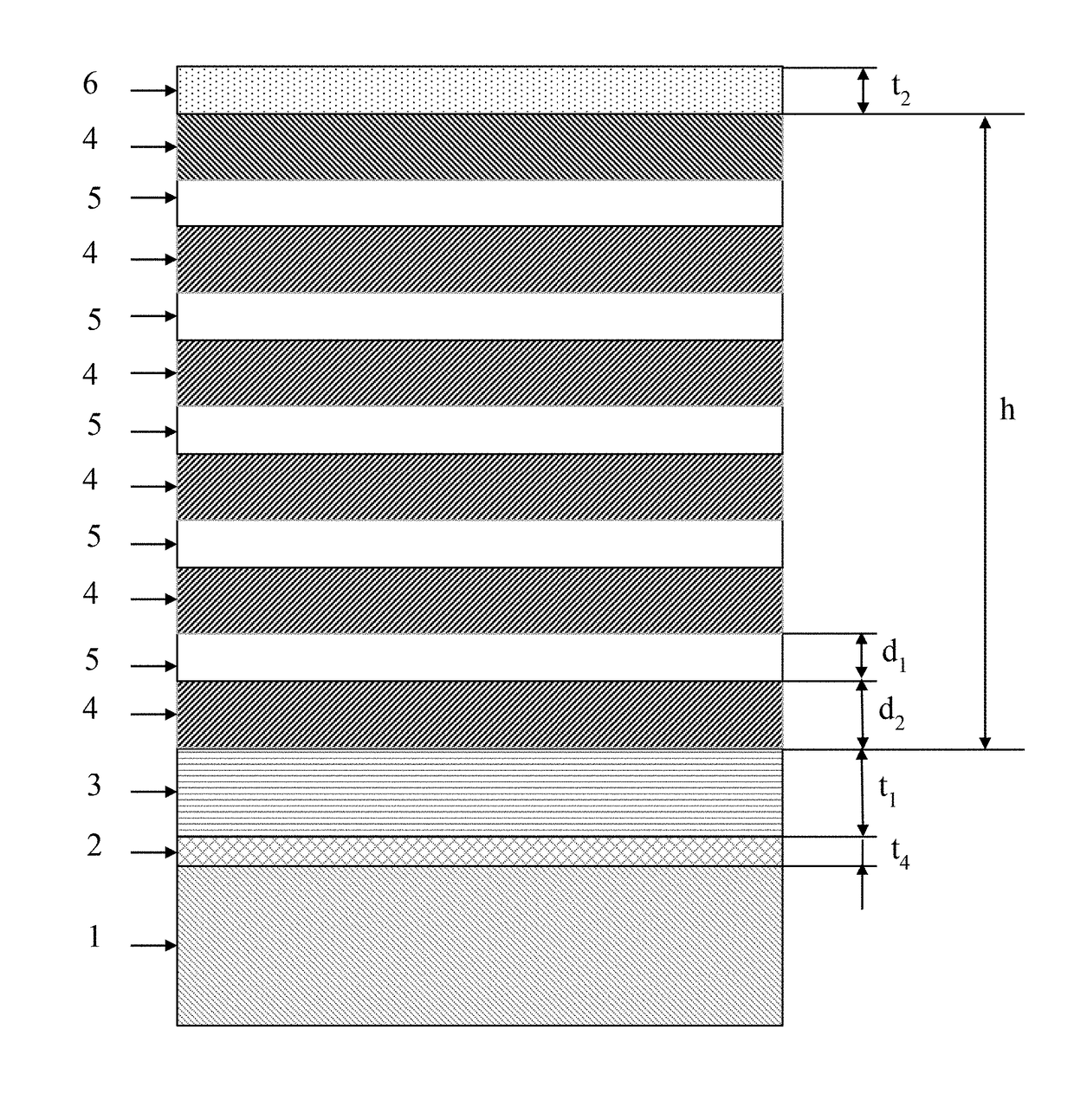
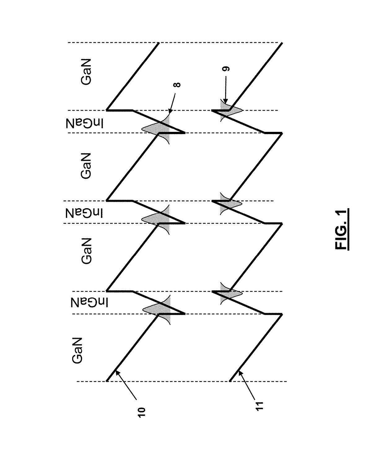
[0029]A part of the scintillator is a multilayer semiconductor nitride heterostructure with a GaN buffer layer 2 prepared with the MOVPE technology. It is essential for the quality and function of the heterostructure active area that the AlybInxbGa1-xb-ybN barrier layer 4 in the active area is lattice matched to the GaN buffer layer in the epitaxial plane and, simultaneously, that the AlywInxwGa1-xw-ywN layers 5 with a narrower band gap representing potential wells have the same polarisation as the barrier layers 4. The AlybInxbGa1-xb-ybN barrier layer 4 must contain approximately 4.3× more Al atoms than In atoms (yb=4.3·xb), so that it could be lattice matched to the buffer layer.

[0030]The heterostructure is prepared on the YAP (yttrium-aluminium perovskite) substrate 1 with orientation (111). After the preparation, the nitridation was performed of the substrate 1 in the NH3+N2 atmosphere at the temperature of 1050° C. for the period of 5 m...

example 2

with a Partially Balanced Piezoelectric Field and Fully Compensated Strain in Epitaxial Layers

[0031]The multilayer semiconductor heterostructure was prepared according to Example 1 and the composition and thickness d2 of the barrier layer 4 with a smaller lattice constant at, is arranged in such a manner that the strain caused by layer 5 representing a potential well with a larger lattice constant aw and thickness d1 is balanced against the bottom layer 3 with lattice parameter a0, which, in this Example, is created with GaN. Simultaneously, the piezoelectric field is compensated between the layers 4 and layers 5 representing a potential well (both the types have the same polarisation). The active area is created with alternating layers 4 and 5 with a broader and narrower band gaps, prepared at the temperature of 830° C. The number of repetition of the active couples is 30. The parameters of layers 4 and 5 are AlybInxbGa1-xb-ybN, where xb=0, yb=0.15 with the thickness d2 of the laye...

example 4

with an Immersed Carrier Attracting Layer

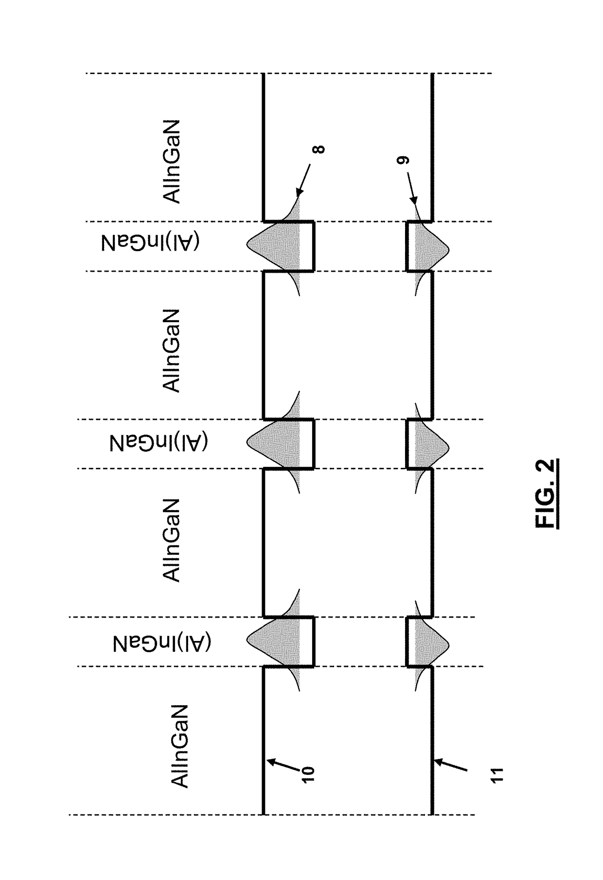
[0033]This structure (ref to FIG. 3 and FIG. 6) is prepared according to Example 1, however, there is inserted in the layer 5 with a narrower band gap with the AlywInxwGa1-xw-ywN composition a thin InxdGa1-xdN layer 7 as the carrier attracting layer which pulls inside itself electrons and holes and thus improves the overlap of the wave functions of the charge carriers also in the case when piezoelectric field is present, therefore it enables to decrease the aluminium concentration in the active area.

[0034]The structure is prepared on the YAP (yttrium-aluminium perovskite) substrate 1 with orientation (111). The nitridation was performed of the substrate 1 in the NH3+N2 atmosphere at the temperature of 1050° C. for the period of 5 minutes. Subsequently, a nucleation layer 2 from the GaN material was prepared at the temperature of 540° C. whose thickness t4 is 30 run. Then the bottom GaN layer 3 was created, doped with silicon atoms to the conc...


PUM


Abstract

A scintillation detector for detecting ionizing radiation, which comprises: a monocrystalline substrate layer; at least one bottom nitride semiconductor layer; an active area on top of the nitride bottom semiconductor layer, which comprises a plurality of alternating nitride semiconductor layers of substantially the same polarization, each couple of the alternating layers consists of a barrier layer of a AlybInxbGa1-xb-ybN type and a potential well layer of a AlywInxwGa1-xw-ywN type for radiant recombinations of electrons and holes, where xb≤xw and yb≤yw is valid; at least one top nitride semiconductor layer on top of the active area; and at least one GaN buffer layer for binding with epitaxy on top of said monocrystalline substrate a structure which comprises: the bottom nitride semiconductor layer; the alternating layers of the active area; and the top nitride semiconductor layer; each of the nitride semiconductor layers has the general formula of AlyInxGa1-x-yN.

Description

FIELD OF THE INVENTION[0001]The invention refers to semiconductor monocrystalline scintillation detectors with nitride heterostructure, designated for the detection of ionising radiation, especially electron, X-ray or particle radiation.BACKGROUND OF THE INVENTION[0002]It is known that semiconductors with a broad band gap, such as GaN or ZnO, are suitable for utilization in detectors of ionising radiation. The materials of this type show a short decay time of excited luminescence in the order of 1 ns and are radiation resistant. The advantage of GaN is the possibility of its preparation in higher crystallographic quality and in the form of homogenous epitaxial layers, applied onto large surfaces of monocrystalline substrates in up to several different layers on top of each other which results in the creation of heterostructures. These heterostructures show low non-radiant losses and a narrow luminescence maximum.[0003]The patent document U.S. Pat. No. 7,053,375 B2 describes a semico...

Claims


Application Information

Patent Timeline
Patent Type & Authority Patents(United States)
IPC IPC(8): G01T1/29G01T1/164G01T1/24H01J37/244H01J49/02G01T1/202
CPCG01T1/2985G01T1/1644G01T1/2023H01J37/244H01J49/025G01T1/24H01J2237/2443G01T1/20
Inventor HOSPODKOVA, ALICEBLA{CIRCUMFLEX OVERHULICIUS, EDUARDTOUS, JANNIKL, MARTIN
Owner CRYTUR SPOL SRO
Why Eureka
Try Eureka