Microwave annealing of flowable oxides with trap layers

a flowable oxide and microwave annealing technology, applied in the direction of semiconductor devices, electrical equipment, transistors, etc., can solve the problems of incompatibility of density annealing, incompatibility of steam processing with materials, and inability to cure oxides, etc., to achieve the effect of increasing the density of the cured insulator

Inactive Publication Date: 2019-02-19
GLOBALFOUNDRIES US INC
View PDF4 Cites 2 Cited by
  • Summary
  • Abstract
  • Description
  • Claims
  • Application Information

AI Technical Summary

Benefits of technology

[0007]Following the curing process (and possible formation of intervening second insulator layers), these methods select wavelengths of microwave radiation (that will be subsequently used during annealing) so that such wavelengths excite the nitrogen, hydrogen, nitrogen monohydride, or hydroxyl-rich atomic clusters. Then, these methods anneal the cured insulator by exposing the cured insulator to microwave radiation in an inert (e.g., non-oxidizing) ambient atmosphere, at a temperature below 500° C., so as to increase the density of the cured insulator. Subsequently, these methods remove portions of the cured insulator after the annealing, to leave the cured insulator only in the trenches.

Problems solved by technology

); however, such densification anneals may be incompatible with manufacturing flows that limit temperatures to less than 500° C., and manufacturing flows that perform oxidization.
Thus, such steam processing may be incompatible with materials such as SiGe, metals (e.g., work function metals) and materials that must be processed at lower temperatures, such as glass, ceramic, or organic substrates used for internet of things (IoT), flexible electronics such as silicon on insulator (SOI), etc.
Additionally, aggressively scaled fin-type field effect transistors (FINFETs) with narrow fins (e.g., less than 10 nm wide) could be undesirably oxidized during steam annealing processes, necessitating the use of liners such as polysilicon and nitride that adversely impact the filling of gaps.

Method used


Image

  • Microwave annealing of flowable oxides with trap layers
  • Microwave annealing of flowable oxides with trap layers
  • Microwave annealing of flowable oxides with trap layers

Examples


Embodiment Construction

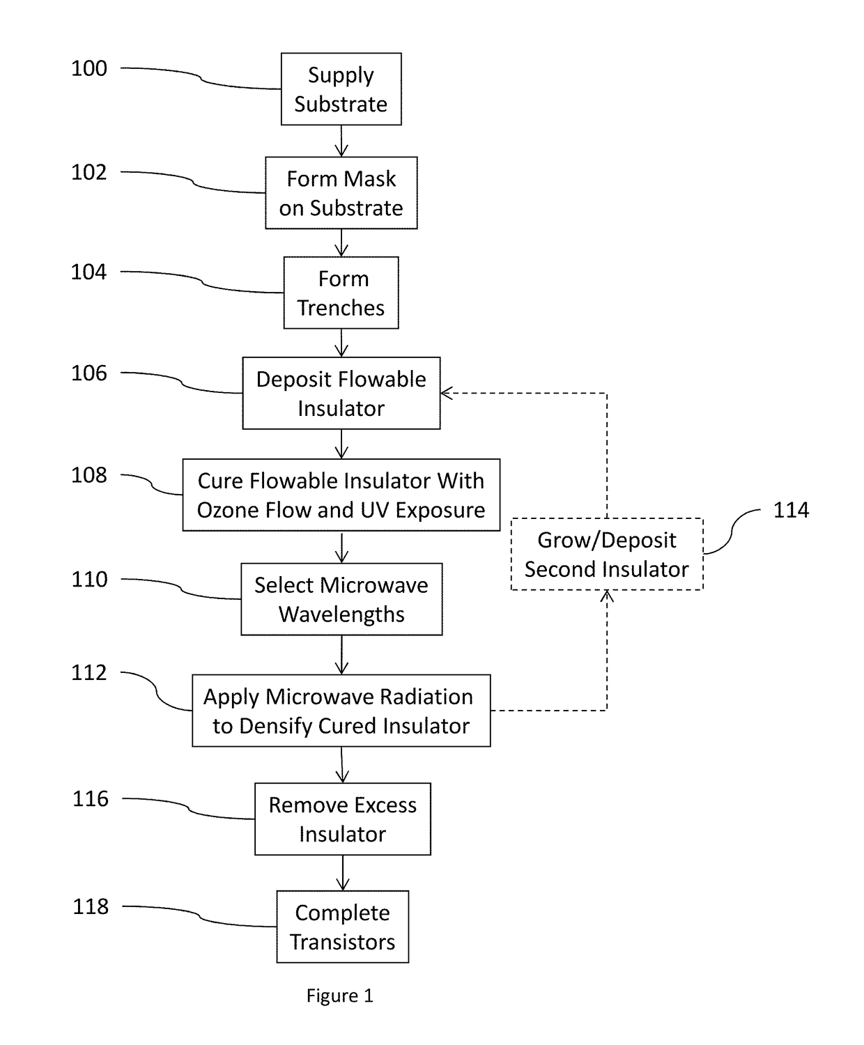
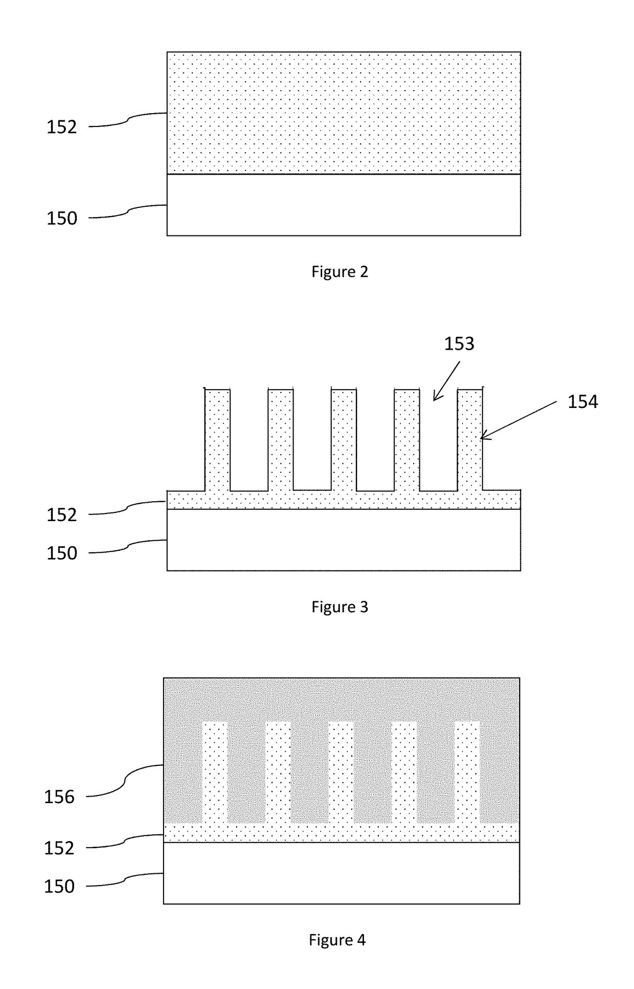
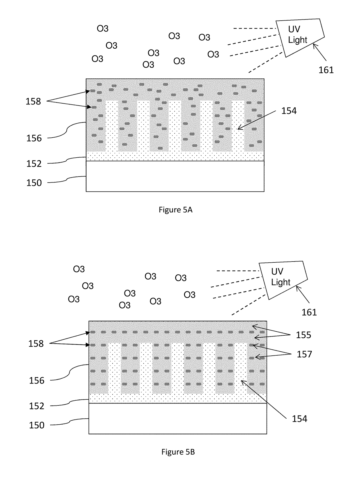
[0018]As noted above, the annealing processes used for densification of flowable oxides can be incompatible with manufacturing flows that require temperatures to remain below a temperature limit (e.g., 500° C., etc.). In view of this, the methods and systems herein convert the flowable insulator formed in the flowable chemical vapor deposition (FCVD) processing to SiO2 at temperatures below 500° C. (e.g., 250° C.-300° C.), without using an oxidizing steam anneal (and without affecting wet etch rates).

[0019]More specifically, the methods and systems herein reduce the temperature used for flowable oxide densification to below 500° C. by forming trap layers (e.g., nitrogen rich atomic clusters), and coupling later applied microwave energy to these trap layers. For example, such dielectrics are useful for STI and ILD applications, as well as middle of line (MOL) gap fill structures, where a non-oxidizing ambient is beneficial (in addition to a thermally restricted flow).

[0020]This discl...


PUM


Abstract

An insulator is formed by flowable chemical vapor deposition (FCVD) process. The insulator is cured by exposing the insulator to ultraviolet light while flowing ozone over the insulator to produce a cured insulator. The curing process forms nitrogen, hydrogen, nitrogen monohydride, or hydroxyl-rich atomic clusters in the insulator. Following the curing process, these methods select wavelengths of microwave radiation (that will be subsequently used during annealing) so that such wavelengths excite the nitrogen, hydrogen, nitrogen monohydride, or hydroxyl-rich atomic clusters. Then, these methods anneal the cured insulator by exposing the cured insulator to microwave radiation in an inert (e.g., non-oxidizing) ambient atmosphere, at a temperature below 500° C., so as to increase the density of the cured insulator.

Description

BACKGROUNDField of the Invention[0001]The present disclosure relates to integrated circuit structures and the manufacture thereof, and more specifically, to microwave annealing of flowable oxides with trap layers.Description of Related Art[0002]Integrated circuit devices use transistors for many different functions, and these transistors can take many different forms, from planar transistors, to vertical transistors, to transistors that use a “fin” style structure. Generally, transistor structures are formed by depositing or implanting impurities into a substrate or fin to form at least one semiconductor channel region, bordered by shallow trench isolation regions below the top (upper) surface of the substrate. A “substrate” can be any material appropriate for the given purpose (whether now known or developed in the future) and can be, for example, silicon-based wafers (bulk materials), ceramic materials, organic materials, oxide materials, nitride materials, etc., whether doped or ...

Claims


Application Information

Patent Timeline
Patent Type & Authority Patents(United States)
IPC IPC(8): H01L21/02H01L21/3105H01L29/06H01L21/762H01L27/088
CPCH01L21/02271H01L21/3105H01L29/0653H01L21/76224H01L27/0886H01L21/02164H01L21/02219H01L21/02345H01L21/02348H01L21/823431
Inventor KRISHNAN, RISHIKESHKASSIM, JOSEPH K.KRISHNAN, BHARAT V.SHEPARD, JR., JOSEPH F.LEE, RINUS TEK POXU, YIHENG
Owner GLOBALFOUNDRIES US INC
Why Eureka
Try Eureka