Fabrication of semi-polar crystal structures

a technology of semi-polar crystal structures and crystal structures, which is applied in the direction of crystal growth process, chemically reactive gases, electrical equipment, etc., can solve the problems of piezoelectric electric fields, general illumination consumes 19% of the total energy consumption of the world, and unparallel impa

Inactive Publication Date: 2019-05-14
SEREN PHOTONICS
View PDF11 Cites 0 Cited by
  • Summary
  • Abstract
  • Description
  • Claims
  • Application Information

AI Technical Summary

Problems solved by technology

The last four decades have seen an unparalleled impact on semiconductor industry generated by silicon technology, accounting for over 90% of the global semiconductor market.
General illumination consumes 19% of the world's total energy consumption.
This generates a polarization issue, thus leading to piezoelectric electric fields.
As a result devices exhibit a reduced overlap between the electron and hole wavefunctions, leading to a long radiative recombination time and thus low quantum efficiency.
The growth of GaN on silicon (i.e. GaN-on-Si technology) is coming up, but is also limited to polar c-plane GaN.
The material issues which result from using the GaN-on-Si technology become even more severe compared with GaN-on-sapphire.
However, the results are far from satisfactory due to a number of challenges which are heavily restricting development of semi / non polar GaN on silicon.
Unlike sapphire substrates, it is extremely difficult to obtain non / semi-polar GaN on any planar silicon substrate.
This is due to a strong chemical reaction between the grown GaN and silicon, leading to a poor surface morphology and eventually growth collapse.
However, for the growth on the patterned (113) silicon with the inclined strips, unavoidably a large number of residual voids are generated during the growth, leaving the grown GaN to directly contact silicon (see FIG. 1).
As a result, the crystal quality is far from satisfactory.
However, the approach had some problems.
First, the melting-back issue has not yet been solved.
This has proved extremely difficult.

Method used


Image

  • Fabrication of semi-polar crystal structures
  • Fabrication of semi-polar crystal structures

Examples


Embodiment Construction

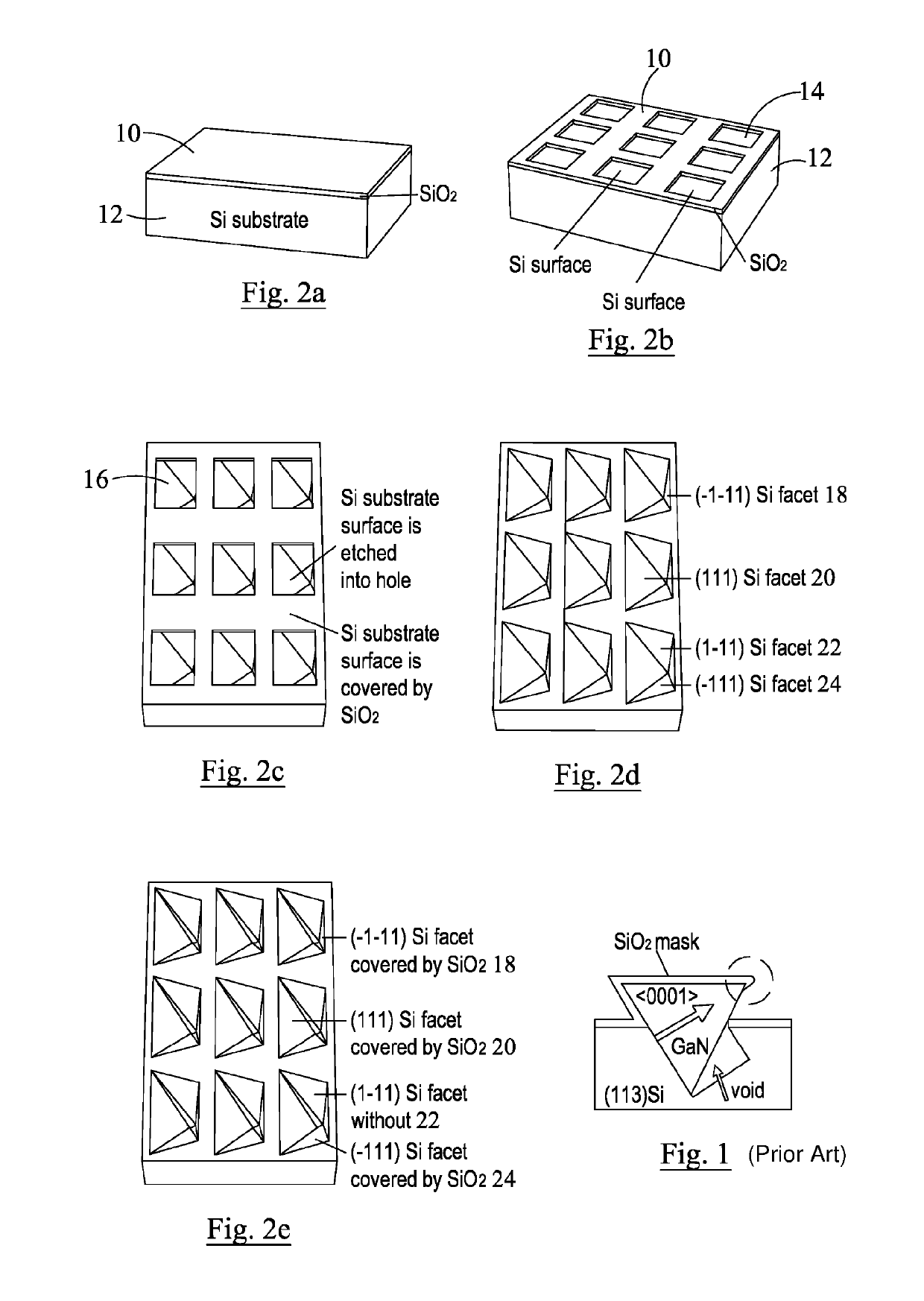
[0024]Referring to FIGS. 2a to 2e a method for the fabrication of an atomically flat (11-22) GaN template on (113) silicon will now be described. Firstly a (113) silicon substrate, i.e. a silicon substrate having a flat surface in the (113) plane of its crystal structure, is provided. As shown in FIG. 2a, a SiO2 thin film 10 is deposited on the surface of the (113) silicon substrate 12 by plasma-enhanced chemical vapour deposition (PECDV). In other embodiments the SiO2 may be deposited using electron-beam evaporator or sputtering deposition. Then, as shown in FIG. 2b, an array of windows 14, in this embodiment a regular square array of 2×2 μm size square windows (though, the window size could be smaller or larger from 500×500 nm to 10×10 μm) with a separation, of about 1 μm (though the separation could be from 100 nm to 5 μm), are opened across the whole wafer using a standard photolithography and dry etching technique (in this case reactive ion etching RIE) to etch through the SiO2...


PUM

PropertyMeasurementUnit
sizeaaaaaaaaaa
sizeaaaaaaaaaa
sizeaaaaaaaaaa

Abstract

A method of growing a group III nitride crystal structure comprises: providing a silicon substrate (12); forming a first mask (10) on the substrate, the mask having a plurality of apertures (14) through it each exposing a respective area of the silicon substrate; etching the silicon exposed by each of the apertures to form a respective recess (16) having a plurality of facets (18, 20, 22, 24); depositing a second mask over some of the facets of each recess leaving at least one of the facets (22) of each recess exposed; and growing group III nitride on the exposed facets (22) and then over the substrate to form a continuous layer.

Description

FIELD OF THE INVENTION[0001]The present invention relates to the growth of non-polar and semi-polar crystal structures, and templates including such structures. It has particular application in the growth of semi-polar or non-polar GaN on silicon, but can also be used for other group III nitrides, such as semi-polar aluminium nitride (AlN), semi-polar aluminium gallium nitride (AlGaN), or semi-polar indium gallium nitride (InGaN).BACKGROUND TO THE INVENTION[0002]The last four decades have seen an unparalleled impact on semiconductor industry generated by silicon technology, accounting for over 90% of the global semiconductor market. Given the mature and cost-effective technology based on silicon, the unification of Group III-V technologies with silicon technology has potential to provide a very good solution to the integration of semiconductor based electronics and photonics. General illumination consumes 19% of the world's total energy consumption. Due to a significantly increasing...

Claims


Application Information

Patent Timeline
Patent Type & Authority Patents(United States)
IPC IPC(8): C30B25/02H01L21/02H01L21/308H01L29/20
CPCH01L21/02639H01L21/0243H01L21/0254H01L21/02381H01L21/02433H01L29/2003H01L21/02609H01L21/02647H01L21/02658H01L21/308H01L21/02458
Inventor WANG, TAO
Owner SEREN PHOTONICS
Why Eureka
Try Eureka