Low-contrast metasurfaces

a metasurface and low-contrast technology, applied in the field of low-contrast metasurfaces, can solve the problems of titanium oxide lacking cmos compatibility, imposing a fundamental limitation on the miniaturization of optical sensors and elements, and metal loss at optical frequencies significant,

Active Publication Date: 2019-07-30
UNIV OF WASHINGTON
View PDF14 Cites 6 Cited by
  • Summary
  • Abstract
  • Description
  • Claims
  • Application Information

AI Technical Summary

Benefits of technology

[0004]Accordingly, new metasurface designs and compositions are needed in order to ac

Problems solved by technology

This imposes a fundamental limitation on the miniaturization of optical sensors and elements, which is necessary for various applications such as the Internet of Things, bio-photonics and two photon absorption microscopy.
Unfortunately, metals are significantly lossy at optical frequencies, titanium oxide lacks CMOS compatibility, and amorphous silicon absorbs light in the

Method used


Image

  • Low-contrast metasurfaces
  • Low-contrast metasurfaces
  • Low-contrast metasurfaces

Examples


example 1

ast Dielectric Metasurface Optics

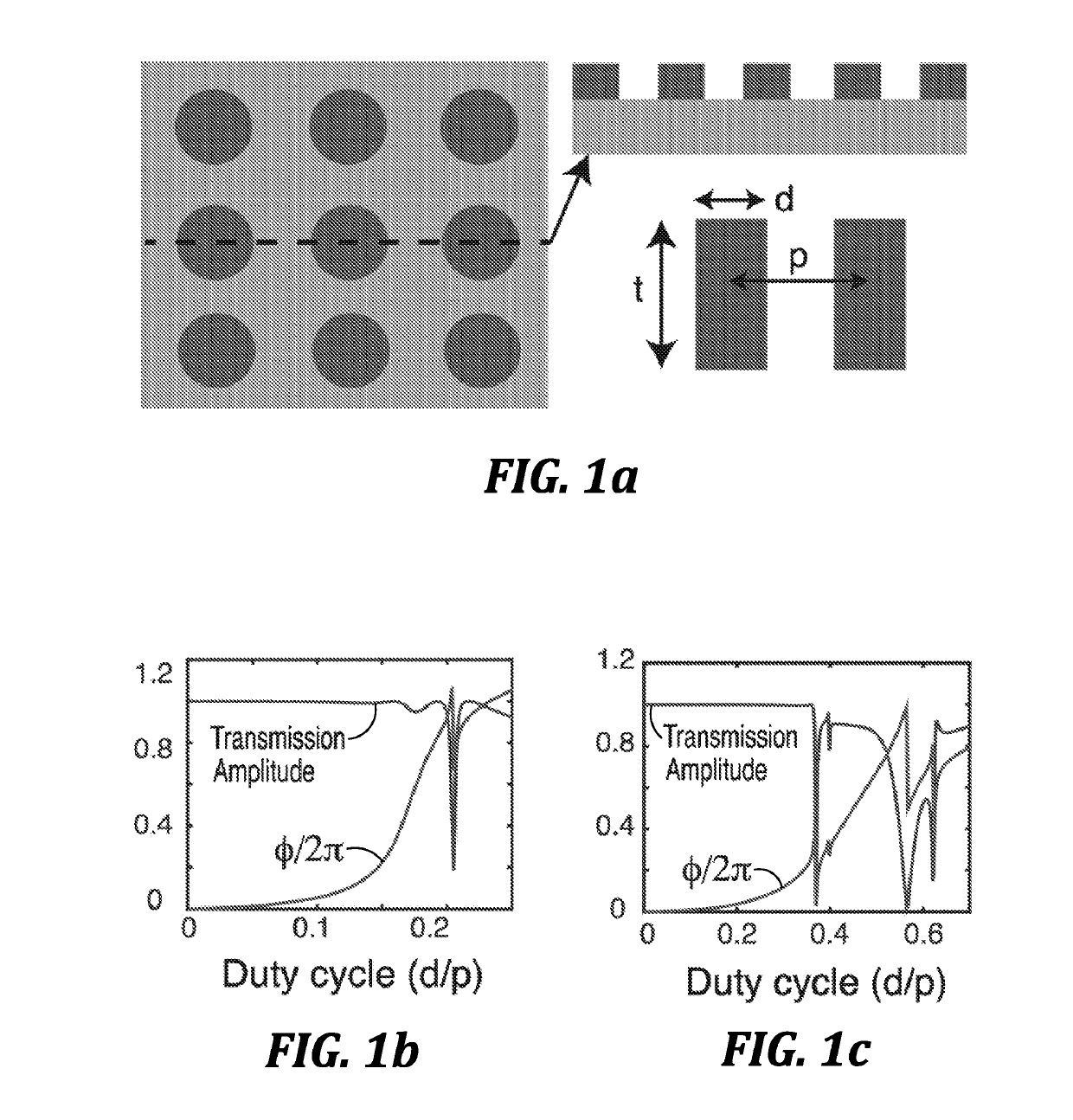
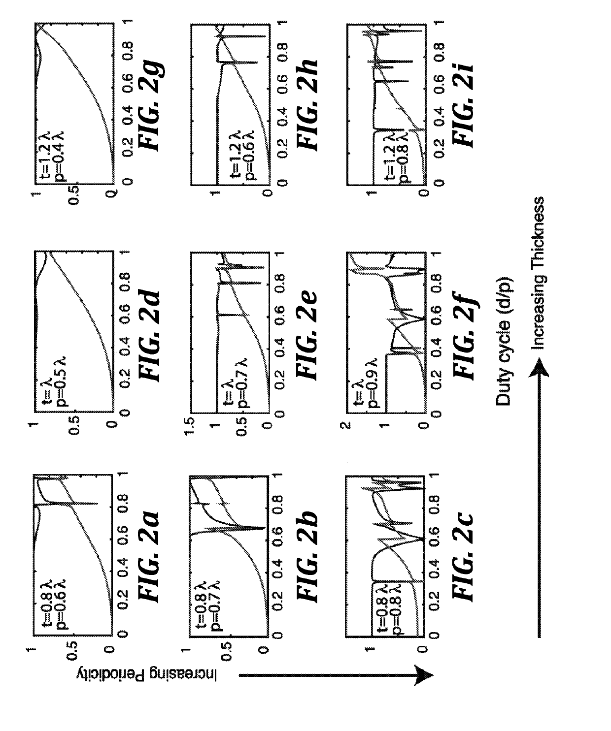
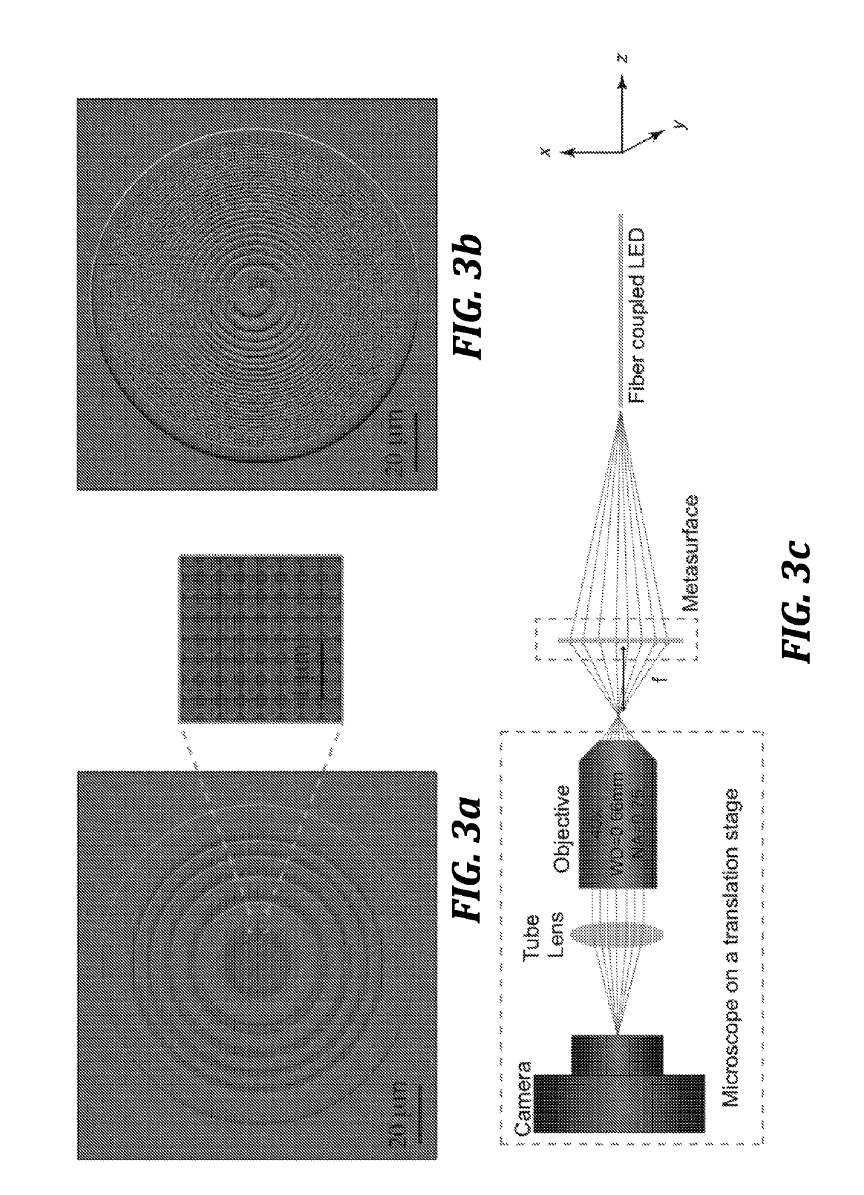
[0087]The miniaturization of current image sensors is largely limited by the volume of the optical elements. Using a sub-wavelength patterned quasi-periodic structure, also known as a metasurface, one can build planar optical elements based on the principle of diffraction. However, recent demonstrations of high quality metasurface optical elements are mostly based on high refractive index materials. Here, we present a design of low contrast metasurface-based optical elements. We validate our theory by fabricating and experimentally characterizing several silicon nitride based lenses and vortex beam generators. The fabricated lenses achieved beam spots of less than 1 μm with numerical apertures as high as ˜0.75. A transmission efficiency of 90% and focusing efficiency of 40% in the visible regime was observed. Our results pave the way towards building low loss metasurface-based optical elements at visible frequencies using low contrast materials, and ...

example 2

ce Analogue of Freeform Optical Designs

[0111]Freeform optics aims to expand the toolkit of optical elements by allowing for more complex phase geometries beyond rotational symmetry. Complex, asymmetric curvatures are employed to enhance the performance of optical components while minimizing their weight and size. Unfortunately, these high curvatures and complex forms are often difficult to manufacture with current technologies, especially at the micron scale. Metasurfaces are planar sub-wavelength structures that can control the phase, amplitude, and polarization of incident light, and can thereby mimic complex geometric curvatures on a flat, wavelength-scale thick surface. We present a methodology for designing analogues of freeform optics using a low contrast dielectric metasurface platform for operation at visible wavelengths. We demonstrate a cubic phase plate with a point spread function exhibiting enhanced depth of field over 300 μm along the optical axis with potential for pe...


PUM


Abstract

Disclosed herein are metasurfaces formed on a substrate from a plurality of posts. The metasurfaces are configured to be optically active at one or more wavelengths and in certain embodiments are configured to form lenses having unexpectedly strong focusing power. In particular, the metasurfaces are formed from “low-contrast” materials, including CMOS-compatible materials such as silicon dioxide or silicon nitride. Accordingly, the disclosed metasurfaces are generally CMOS compatible and therefore embody a new paradigm in metasurface design and manufacturing.

Description

CROSS-REFERENCES TO RELATED APPLICATIONS[0001]This application claims the benefit of U.S. Patent Application No. 62 / 215,518, filed Sep. 8, 2015, and of U.S. Patent Application No. 62 / 342,121, filed May 26, 2016, the disclosures of which are hereby incorporated by reference in their entirety.BACKGROUND[0002]Conventional transmissive macroscopic optical elements primarily depend on refraction to control the propagation of light. Refraction relies heavily upon the exact curvature of the surface, and the spatial extent of the element in order to achieve gradual phase accumulation. This imposes a fundamental limitation on the miniaturization of optical sensors and elements, which is necessary for various applications such as the Internet of Things, bio-photonics and two photon absorption microscopy. Metasurfaces, two-dimensional quasi-periodic arrays of sub-wavelength structures, present a method of miniaturizing optical elements. Rather than relying on gradual phase accumulation through...

Claims


Application Information

Patent Timeline
IPC IPC(8): G02B5/18G02B1/00
CPCG02B5/1871G02B1/002G02B5/1828G02B5/1876G02B5/1814G02B2005/1804G02B5/1809
Inventor ZHAN, ALANCOLBURN, SHANEMAJUMDAR, ARKA
Owner UNIV OF WASHINGTON
Why Eureka
Try Eureka