Silicon-based photodetectors with expanded bandwidth

Active Publication Date: 2019-09-03
UNIV OF MARYLAND
View PDF3 Cites 3 Cited by
  • Summary
  • Abstract
  • Description
  • Claims
  • Application Information

AI Technical Summary

Benefits of technology

[0018]It is an object of the present invention to provide a silicon-based photosensor which is easily integrated into commercial Si devices while abso

Problems solved by technology

When high frequency electromagnetic radiation is involved, the functionality of the metal becomes more complex and obey plasmonics principles.
However, ohmic losses which originate in the cooling of excited (or so-called “hot”) carriers, have kept many devices from being developed and have led to a search for alternative materials.
These oscillations are typically confined to a small volume and result in high field intensities.
However, these metamaterials require complicated and costly nanofabrication techniques making them difficult to commercialize.
While zeroth order FP cavities have been used to increase absorpt

Method used


Image

  • Silicon-based photodetectors with expanded bandwidth
  • Silicon-based photodetectors with expanded bandwidth
  • Silicon-based photodetectors with expanded bandwidth

Examples


Embodiment Construction

)

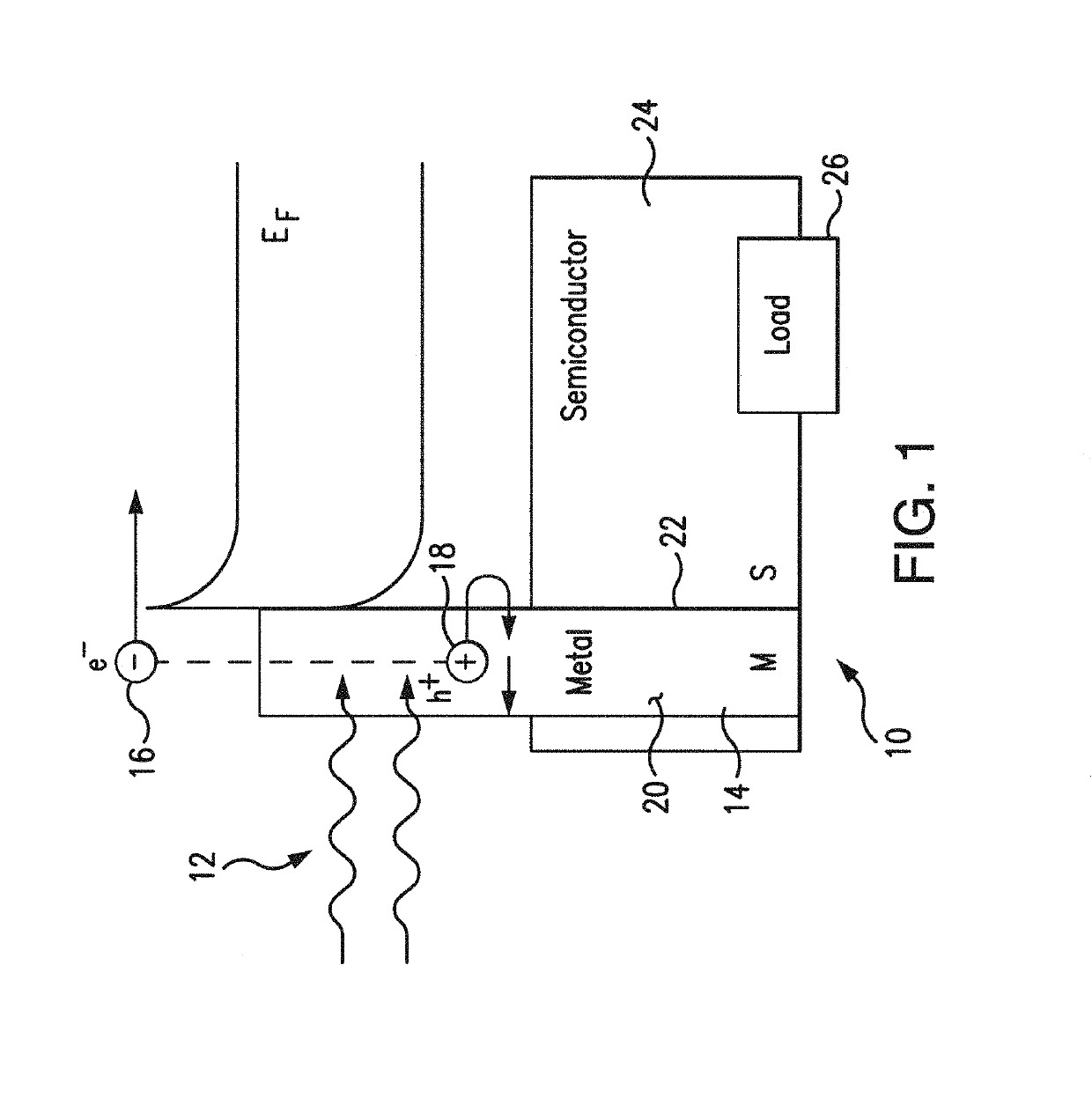
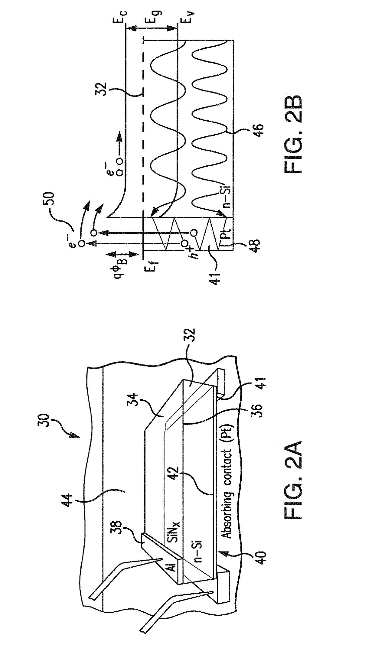
[0056]Production of metal excited electron-hole pairs which lead to photo generation has been observed in a Metal-Semiconductor hot plasmonic structure 10, shown in FIG. 1, which is based on a Schottky interface with a semiconductor, for example, silicon (Si) when light 12 is incident on a metal film 14 in the Schottky contact. The photon-induced electron emission has been attained across the Schottky junction formed at a metal-semiconductor interface. It is shown that sub-bandgap photons 12 are absorbed in the metal 14 and lead to photogenerated current.

[0057]For absorption of the light 12 in the metal 14, an electron 16 in the Fermi gas absorbs a photon and is excited to a higher energy state. These excited “hot” electrons 16 leave an empty state in the Fermi gas, generating “hot” holes 18. The “hot” carriers 16, 18 travel within the metal 14 and are subjected to scattering that results in the carriers' relaxation and recombination.

[0058]At Infrared (IR) and optical frequencies, ...


PUM


Abstract

A hot carrier photodetector has been developed that absorbs approximately 80% of broadband infrared radiation by using a planar nanoscale back metal contact to silicon. Based on the principles of the hot carriers generation in ultrathin metal films, silicon-based CMOS image sensors are developed which operate in the IR diapason. The device uses absorption in an ultrathin metallic nanostructure to generate therein a non-equilibrium electron distribution which subsequently is injected into the silicon material via a Schottky contact at the Si body, thus generating a photoresponse to an incident IR radiation. A pixeled array including interconnected hot carriers metallic nanostructured cell(s) and traditional RGB elements is envisioned to enable RGB-IR imaging from a single silicon based wafer.

Description

REFERENCE TO RELATED APPLICATIONS[0001]This Utility Patent Application is based on the Provisional Patent Application 62 / 344,126 filed on 1 Jun. 2016.FIELD OF THE INVENTION[0002]The present invention is directed to silicon (Si) based photodetectors, and particularly, to silicon-based photodetectors capable of operating in the Infrared (IR) spectrum.[0003]More in particular, the present invention is directed to infrared silicon-based photodetectors utilizing hot carriers generation in an ultrathin metal contact formed at the silicon body which absorbs about 80% of broadband radiation to produce photocurrent.[0004]The present invention is also directed to silicon-based CMOS (Complementary Metal-Oxide-Semiconductor) image sensors capable of operating in the infrared diapason zone based on absorption from a thin metallic nanostructure formed in contact with the Si body to generate a photoresponse to the incident light using a non-equilibrium hot electron distribution which is injected i...

Claims


Application Information

Patent Timeline
IPC IPC(8): H01L27/15H01L31/0224H01L31/108H01L31/07H01L31/105H01L29/06H01L31/02
CPCH01L31/105H01L27/15H01L31/1085H01L29/0619H01L31/02024H01L31/022416H01L31/07H01L31/108Y02E10/50
Inventor MUNDAY, JEREMY NATHAN
Owner UNIV OF MARYLAND
Why Eureka
Try Eureka