Capacitive matrix arrangement and method for actuation thereof

a technology of capacitive matrix and actuation method, which is applied in the field of microelectronics, can solve the problems of neighboring cells being parasiticly interfering with neighboring cells, affecting the application of capacitive matrix, and affecting the material wear and storage tim

Active Publication Date: 2019-12-10
SEMRON GMBH
View PDF23 Cites 0 Cited by
  • Summary
  • Abstract
  • Description
  • Claims
  • Application Information

AI Technical Summary

Benefits of technology

[0022]The invention described here makes possible the control of a capacitive coupling in a matrix arrangement. Hence, a field can be generated at one point for actuation purposes and measured at the same time. This actuation occurs without transistors, which combines the benefits of the passive matrix with benefits of the active matrix. In regard to storage technologies, the benefit of the NAND architecture with its high storage density and the benefit of the NOR architecture with high access speed are combined. The storage density amounts to 4F2, as in the case of a passive matrix or the NAND architecture, and the high access speed results from the use of metallic bit lines and reference electrodes, which have a lower resistance than transistors, so that the time constant for the charging of the bit line and the reference electrodes is reduced.
[0029]In order to prevent a complete word line from always having to be depleted or enriched in charge carriers, which is energy and time consuming, in another embodiment it is provided that the strip reference electrodes and the bit lines cross each other and at the crossing points the strip reference electrode is connected to the word line across the p-doped region and the bit line across the n-doped region or the strip reference electrode is connected across the n-doped region and the bit line across the p-doped region, respectively. This also avoids having to separately adjust the Debye-length change and the voltage between reference electrode and bit line.
[0033]Multiple matrix arrangements may also be stacked one on the other according to the invention, whereby the strip reference electrodes may at the same time form the bit lines for the cell situated on top. This arrangement is primarily advantageous for storage applications, since the storage density could be significantly increased in this way.
[0061]Furthermore, a current flow through the word line being selected may produce a slight temperature rise and a metal-insulator junction may trigger a change in the mobile charge carrier concentration in the word line being selected.

Problems solved by technology

The major drawback hindering the application of a passive matrix thus far is the fact that the neighboring cells undergo parasitic interference.
Only in organic ferroelectric storages can this principle be used, but this has drawbacks in terms of material wear and storage time (EP 1 316 090 B1; EP 1 798 732 A1; US 2006 / 0046344 A1; US 2002 / 0017667 A1; US 2003 / 0137865 A1).
However, a diode in resistive elements often has the problem that the ON / OFF ratio is too low and in liquid crystal displays poor contrast is achieved.
Furthermore, a diode itself acts as a capacitance and if the elements being actuated are themselves capacitances, as in the case of liquid crystal displays (US 2011 / 0090443 A1) / electronic paper (US 2008 / 0043317 A1) / micro mirror arrays (U.S. Pat. No. 5,583,688) or ferroelectric storages (EP 1 316 090 B1), an actuation is difficult (voltage divider).
The drawbacks are more manufacturing steps and usually a rather high space requirement for storage devices.
The drawbacks of these two different architectures, along with corresponding storage materials, form one of the reasons why thus far there is no universal storage that replaces SRAM, DRAM, flash storage and hard computer disk.
The biggest problem thus far is the scalability and the storage density, since ferroelectric materials are little compatible with silicon-based CMOS logic.
The neurons usually have a sigmoidal transient response for the activation function, so that a rather complicated transistor circuit is often necessary (U.S. Pat. Nos. 3,476,954; 8,694,452), having a high energy consumption and being difficult to produce.

Method used


Image

  • Capacitive matrix arrangement and method for actuation thereof
  • Capacitive matrix arrangement and method for actuation thereof
  • Capacitive matrix arrangement and method for actuation thereof

Examples


Embodiment Construction

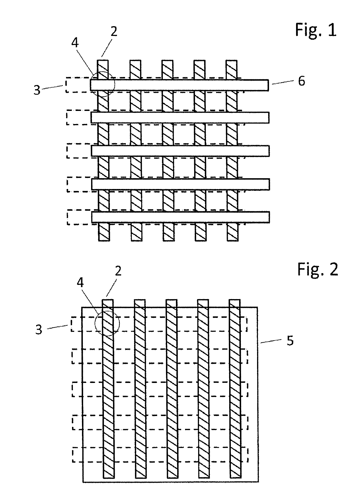
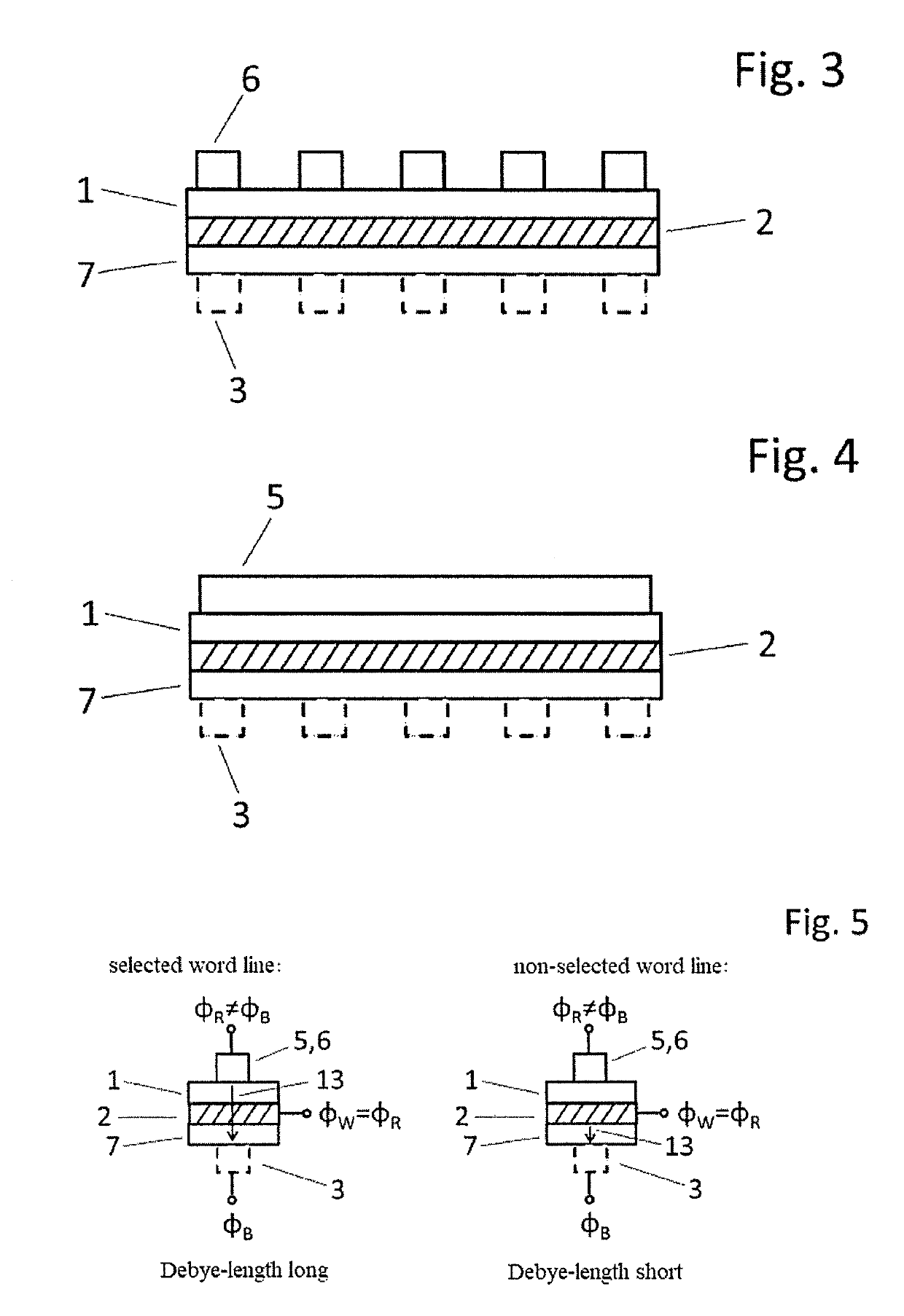
[0081]FIG. 1 to FIG. 4 show a capacitive matrix arrangement, with an active medium 1. The active medium 1 is characterized in that it can be actuated with electric fields, or it may itself possess an electric polarization. The active medium 1 is embedded in a layer between a first set and a second set of respective parallel addressing electrodes, whereby the addressing electrodes of the first set form word lines 2 and the addressing electrodes of the second set form bit lines 3 of the matrix arrangement.

[0082]The word lines 2 and the bit lines 3 intersect at crossing points. At the crossing points, capacitor cells 4 which are selectable by actuation of the word lines 2 and bit lines 3 with the intervening active medium 1 are arranged.

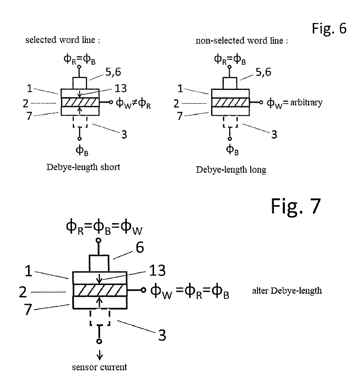
[0083]In the following, ΦR shall describe the potential of the reference electrode 5, 6, ΦB the potential of the bit line 3 and ΦW the potential of the word line 2.

[0084]Now, in order to generate an electric field 13 at one point in the active medium 1 ...


PUM

PropertyMeasurementUnit
Debye lengthaaaaaaaaaa
concentrationaaaaaaaaaa
Fermi levelsaaaaaaaaaa

Abstract

The invention relates to a capacitive matrix arrangement that comprises an active medium, which is arranged in a layer between word lines and bit lines whose crossing points have capacitor cells, selectable by actuation of the word lines and bit lines, arranged at them with the interposed active medium, and to an actuation method, wherein the invention is based on the object of combining active actuation of capacitive elements in a matrix with the advantages of passive actuation. This is achieved by virtue of the word lines having a specific variable Debye length, i.e. consisting of a material with a variable mobile charge carrier concentration, and being arranged between the active medium and a non-active dielectric. The actuation is effected by controlling the action of an electrical field.

Description

CROSS REFERENCE TO RELATED APPLICATIONS[0001]This application is the National Phase filing under 35 U.S.C. § 371 of International Application No.: PCT / EP2017 / 075872, filed on Oct. 10, 2017, and published on Apr. 19, 2018 as WO 2018 / 069359 A1, which claims priority to German Application No.: 10 2016 012 071.1, filed on Oct. 10, 2016 and German Application No.: 10 2017 002 739.0, filed on Mar. 21, 2017. The contents of each of the prior applications are hereby incorporated by reference herein in their entirety.[0002]The invention relates to a capacitive matrix arrangement, comprising an active medium, which is embedded in a layer between a first set and a second set of respective parallel addressing electrodes. The active medium is capable of being actuated by electric fields. It may also itself possess an electric polarization. The addressing electrodes of the first set form word lines and the addressing electrodes of the second set form bit lines of the matrix arrangement. The word ...

Claims


Application Information

Patent Timeline
Patent Type & Authority Patents(United States)
IPC IPC(8): G11C11/22G02B26/00H01L49/02G02F1/167G11C11/54H01L23/532H01L27/11507G02F1/1676G11C11/24G02F1/1343
CPCH01L23/53271H01L28/60G11C11/221G02F1/1676G02F1/167G11C11/2257G02B26/005G11C11/24G11C11/54G02F1/134336H01L27/11507G02F2201/122G11C11/22G06N3/065G06N3/048H10B53/30
Inventor DEMASIUS, KAI-UWEKIRSCHEN, ARON
Owner SEMRON GMBH
Why Eureka
Try Eureka