Optical article and optical filter comprising same

a technology of optical filter and optical article, which is applied in the field of optical article and optical filter, can solve the problems of difficult thinness, easy breakage, and inability to apply to high-resolution camera modules with 5 or more mega pixels, and achieve the effects of suppressing transmittance, preventing ghosting, and high transmittan

Active Publication Date: 2020-09-08
LMS
View PDF9 Cites 1 Cited by
  • Summary
  • Abstract
  • Description
  • Claims
  • Application Information

AI Technical Summary

Benefits of technology

[0013]An optical filter according to the present invention includes an optical article containing one or more types of near-infrared absorbing dyes and having two or more absorption peaks including first and second absorption peaks in the wavelength range from 380 to 1,200 nm, thereby exhibiting high transmittance with respect to light with a wavelength in a visible light range and suppressing transmittance with respect to light with a wavelength range of 800 to 1,000 nm to 0.6% or less. Therefore, the optical filter has advantages in that a ghosting problem can be prevented, a thin image device can be easily manufactured, and production costs can be reduced due to improved yield and productivity in an assembly process.

Problems solved by technology

However, a conventionally used reflective near-infrared shielding filter has a limit in that it cannot be applied to a high-resolution camera module with 5 or more mega pixels since a phenomenon of taking an unintended image (hereinafter, referred to as “ghosting” or “ghost image”) when an image is taken by an imaging device due to internal reflection between an optical filter and a lens of a solid-state imaging element, particularly, between an optical filter and a CIS microlens.
In addition, a conventional absorbing near-infrared shielding filter has a preferable effect of shielding light in the wavelength range from 800 to 1,000 nm, but due to low durability because of the properties of a material, it is difficult to be manufactured thin and thus is easily breakable.

Method used


Image

  • Optical article and optical filter comprising same
  • Optical article and optical filter comprising same
  • Optical article and optical filter comprising same

Examples


preparation examples 1 to 4

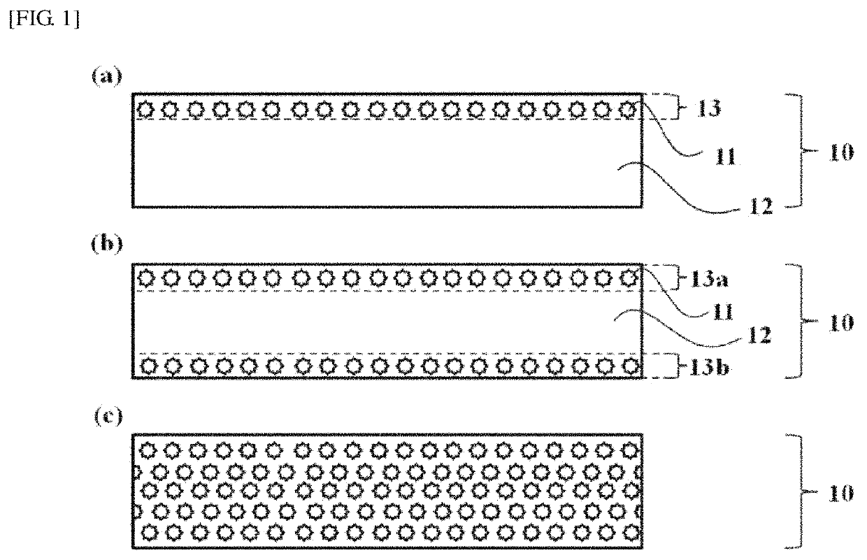
[0105]According to a preparation example of the present invention, an optical article having first and second absorption peaks was prepared as follows.

[0106]A near-infrared absorbent A and a near-infrared absorbent B, which had absorption maximums in the wavelength ranges of 702±5 nm and 905±5 nm, respectively, were mixed at contents shown in Table 1 below with respect to 100 parts by weight of a resin. At this time, as the resin, a polymethylmethacrylate (PMMA) resin was used, and as an organic solvent, cyclohexanone was used. Afterward, the resulting mixture was stirred using a stirrer for 24 hours or more, thereby preparing a near-infrared absorbing solution. The prepared near-infrared absorbing solution was applied to both surfaces of a polyethylene terephthalate (PET) film (A4100, manufactured by Toyobo Co., Ltd.) having a thickness of 0.1 mm, cured at 120° C. for 50 minutes, thereby preparing an optical article having near-infrared absorbing layers on both surfaces thereof as ...

examples 1 to 7

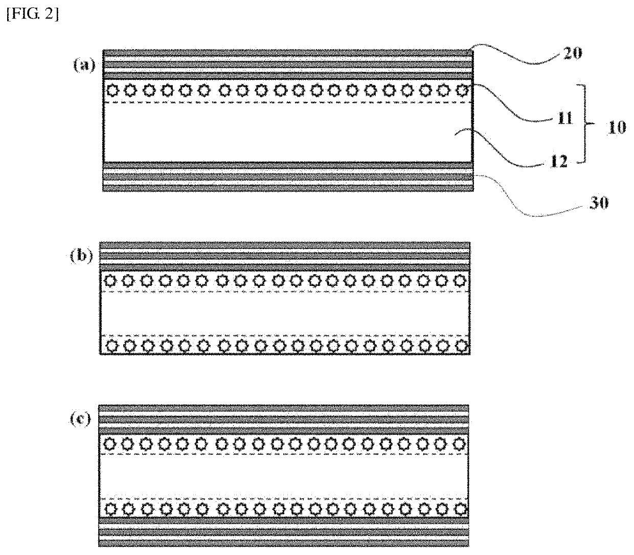
[0109]A first selective wavelength reflection layer having a dielectric multilayer film structure was formed by alternately depositing SiO2 and Ti3O5 on a first main surface of each of the optical articles prepared in Preparation Examples 1 to 4 at 110±5° C. using an E-beam evaporator. Afterward, a second selective wavelength reflection layer having a dielectric multilayer film structure was formed by alternately depositing SiO2 and Ti3O5 on a second main surface of each of the optical articles at 110±5° C. using an E-beam evaporator, resulting in an optical filter having the same structure as shown in FIG. 2C. At this time, the number of stacked layers and thickness of each of the first and second selective wavelength reflection layers are shown in Table 2 below. At this time, the thickness means the total thickness of the first or second selective wavelength reflection layer, and the unit is a micrometer (μm).

[0110]

TABLE 2SecondFirst selectiveselectivewavelengthwavelengthreflectio...

experimental example 1

[0122]To evaluate the transmittance according to an incident angle of the optical filter according to the present invention, an experiment was performed as follows.

[0123]The transmission spectrum for each of the optical filters prepared in Examples 2, 5 to 7 and Comparative Examples 4 to 6 was measured using a spectrophotometer in the wavelength range of 380 to 1,200 nm.

[0124]The transmittances of the visible light and near-infrared rays according to an incident angle were deduced by measuring the transmittances with respect to light (incident angle: 0°) incident in a vertical direction on the optical filter and light (incident angle: 30°) incident in a direction having 30° from the direction perpendicular to the optical filter. The result is shown in Table 7 and FIGS. 7 to 10. At this time, the average transmittance for the visible light refers to a calculated average value of the transmittance per wavelength in the wavelength range of 430 to 565 nm, the average transmittance for t...


PUM

PropertyMeasurementUnit
wavelength rangeaaaaaaaaaa
wavelengthaaaaaaaaaa

Abstract

The present invention relates to an optical article and an optical filter comprising the same. The optical filter comprises an optical article containing one or more near-infrared absorbing dyes and having two or more absorption peaks comprising a first absorption peak and a second absorption peak in a wavelength range of 380 nm to 1,200 nm whereby the optical filter has advantages in that transmissivity is high with respect to light having the wavelength of a visible light region and transmissivity is suppressed to 0.6% or less with respect to light having a wavelength in the range of 800 nm to 1,000 nm so that ghost image problems can be prevented, and a yield and productivity can be improved through the reduction of poor assembly caused by the bending of the optical filter in an image device assembling process.

Description

CROSS REFERENCE TO RELATED APPLICATIONS[0001]This application is a National Phase filing under 35 U.S.C. § 371 of PCT / KR2017 / 001688 filed on Feb. 16, 2017, and claims priority to Korean Patent Application No. 10-2017-0007027 filed on Jan. 16, 2017, and Korean Patent Application No. 10-2016-0021622 filed on Feb. 24, 2016, under 35 U.S.C. § 119. The entire contents of each application are hereby incorporated by reference.TECHNICAL FIELD[0002]The present invention relates to an optical article and an optical filter including the same, and more particularly, to an optical article which can suppress light transmittance in the wavelength range from 800 to 1,000 nm and an optical filter including the same.BACKGROUND ART[0003]To obtain a natural color image as seen by the human eye, an imaging device using a solid-state imaging element such as a CMOS image sensor (CIS) essentially requires an optical article which shields light in the near-infrared range of 800 to 1,000 nm detected by a sen...

Claims


Application Information

Patent Timeline
Patent Type & Authority Patents(United States)
IPC IPC(8): C08K5/01C08K5/00G02B5/22H01L27/146G02B5/26C08L101/00G02B5/20
CPCH01L27/14621C08K5/01C08L101/00G02B5/223C08K5/0041G02B5/208C08K5/0091G02B5/26
Inventor CHOI, JEONG OGJUNG, JOON HOJUNG, JIN HOKIM, JOO YOUNGYANG, SEON HO
Owner LMS
Why Eureka
Try Eureka