

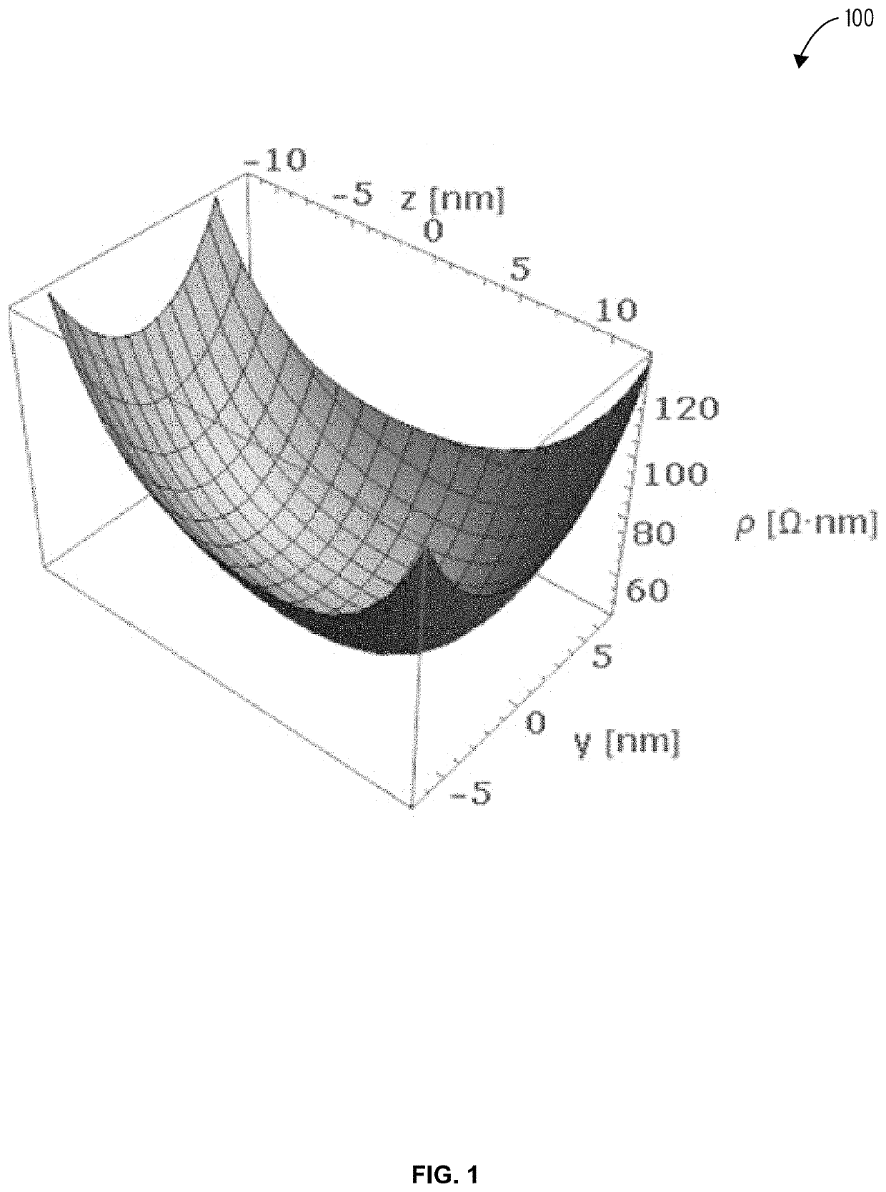
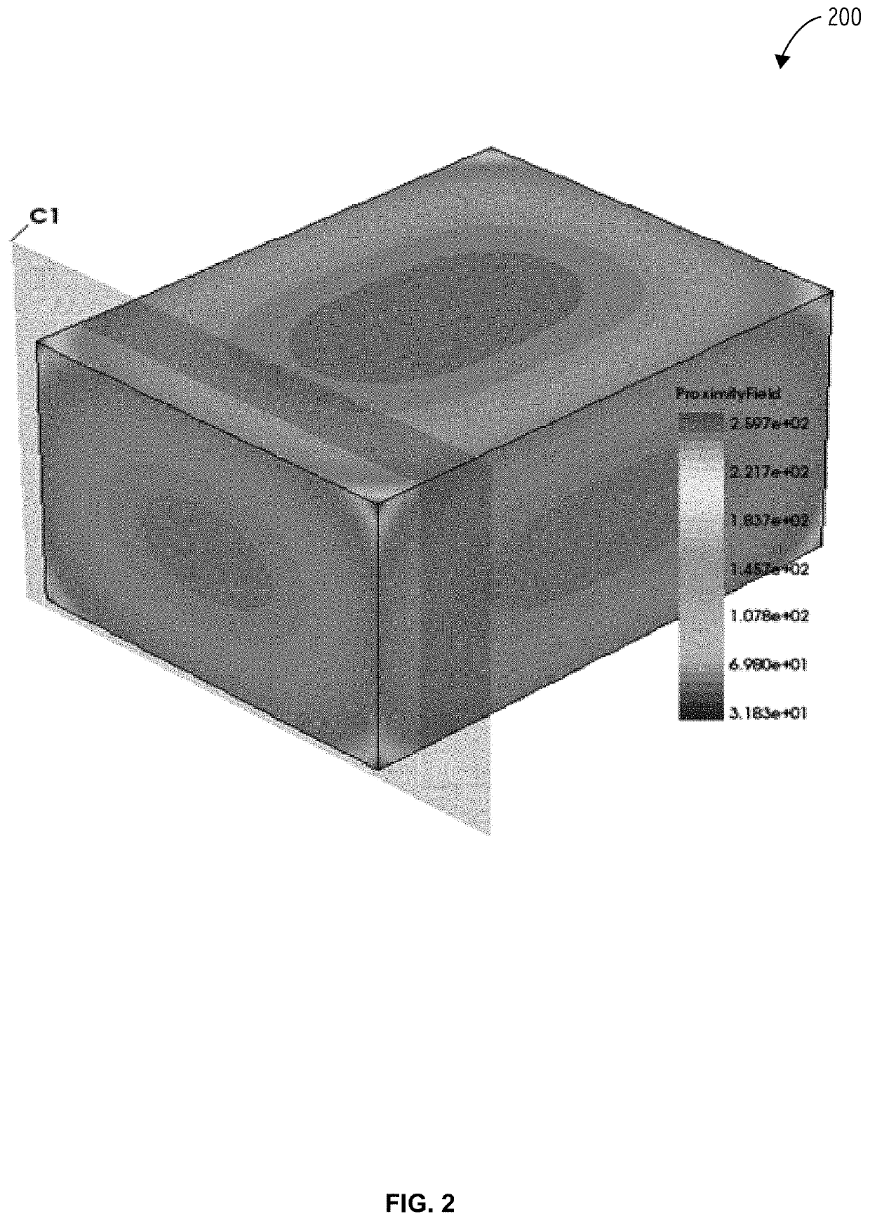
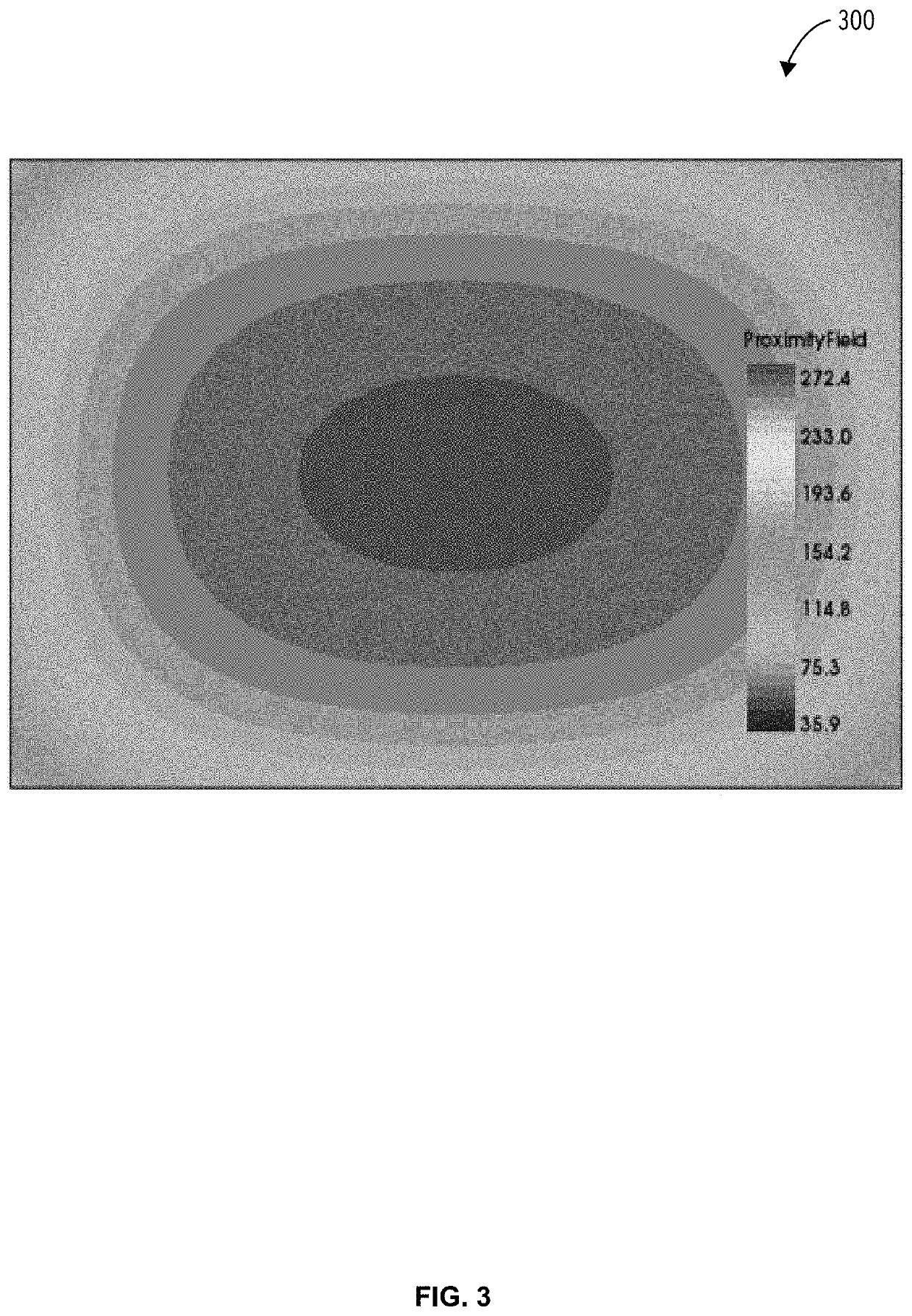
Nano-wire resistance model
a resistance model and nanowire technology, applied in the direction of cad circuit design, instrumentation, semiconductor/solid-state device details, etc., can solve the problems of increasing the cost of ic manufacturing, fewer such wires available, and increasing the delay of signal propagation through the wire, so as to improve the efficiency of timing verification process and improve the reliability of integrated circuits.
- Summary
- Abstract
- Description
- Claims
- Application Information
AI Technical Summary
Benefits of technology
Problems solved by technology
Method used
Image

Examples
Embodiment Construction
[0019]Various terminology is utilized herein, and should be interpreted according to its conventional meaning in the relevant arts, unless otherwise defined below:
[0020]“2D material strip” in this context refers to a length of material that includes fibers or strips that comprise essentially of one or more layers of doped or undoped “2D materials,” such as graphene, phosphorene (PH3) or MoS2 (molybdenum disulfide). A 2D material can be considered to be a material which tends to form strong bonds, such as covalent bonds, in planes with relatively weaker bonds, such as Van der Waals bonds, between the planes like graphene. Strips of 2D materials can be configured in ribbon form (single or multi-layer), nanotube form and woven form, for example.
[0021]“Computer model” in this context refers to the logic (e.g., algorithms and equations) that represent the behavior of the system being modeled. Computer simulation is the actual execution of logic comprising these equations or algorithms. S...
PUM
 Abstract
Description
Claims
Application Information