Compound for organic electric element, organic electric element comprising the same and electronic device thereof
a technology which is applied in the field of organic electric elements and organic electric elements comprising the same, and electronic devices thereof, can solve the problems of insufficient development of stable and efficient host materials for organic electric elements, low charge carrier mobility and low oxidation stability of a 5-membered cyclic compound, and poor effect of polycyclic compound substituents, etc., to achieve the effect of improving the lifetime, reducing the driving voltage of organic electric elements, and improving the luminous efficiency of organi
- Summary
- Abstract
- Description
- Claims
- Application Information
AI Technical Summary
Benefits of technology
Problems solved by technology
Method used
Image
Examples
synthesis example
[0129]The compound (final products) according to the present invention can be synthesized by reacting according to the following method, but are not limited thereto.
[0130]
[0131]R4′ can be the same as the definition of R4, and R4′ meanses a substituent which is the same as R4 or different from R4.
[0132]I. Synthesis of Sub 1
[0133]Sub 1 of the Reaction Scheme 1 can be synthesized according to, but not limited to, the reaction route of the following Reaction Scheme 2 and Reaction Scheme 3.
[0134]
[0135]
[0136]In the above reaction scheme 1, the reactants of
[0137]
were synthesized by referring to four literatures as follows.
[0138]1) The synthesis method disclosed in Korean Patent No. 10-1488560 (Registered on Feb. 3, 2013) filed by Doosan Corporation was used, (See Reaction Scheme A)
[0139]
[0140]2) The synthesis method disclosed in international published patent PCT / EP2015 / 068240 (First priority Filing date: Aug. 8, 2014) filed by BASF was used. (See Reaction Scheme B)
[0141]
[0142]3) The synth...
example 1
[Example 1] Red OLED (Phosphorescent Host)
[0367]Organic light emitting diodes (OLEDs) were fabricated according to a conventional method by using a compound obtained by synthesis as host material of a light emitting.
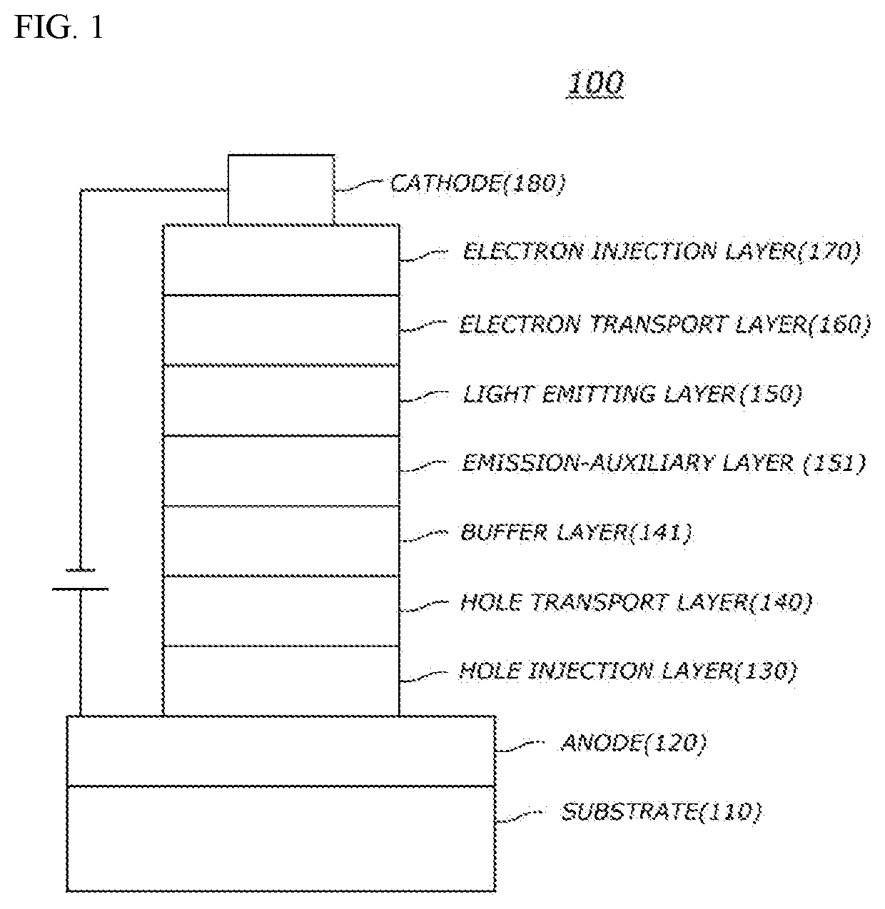
[0368]First, an ITO layer (anode) was formed on a glass substrate, and a film of N1-(naphthalen-2-yl)-N4,N4-bis(4-(naphthalen-2-yl(phenyl)amino)phenyl)-N1-phenylbenzene-1,4-diamine (hereinafter abbreviated as “2-TNATA”) was vacuum-deposited on the ITO layer to form a hole injection layer with a thickness of 60 nm. Then, 4,4-bis[N-(1-naphthyl)-N-phenylamino]biphenyl (hereinafter abbreviated as “NPD”) was vacuum-deposited on the hole injection layer to form a hole transfer layer with a thickness of 60 nm.
[0369]Subsequently, a light emitting layer with a thickness of 30 nm was deposited on the hole transport layer by doping the hole transport layer with the compound 1-1 of the present invention as host material and bis-(1-phenylisoquinolyl)iridium(III)acetylacetonate (herei...
example 44
[Example 2] to [Example 44]
[0372]OLEDs were manufactured in the same manner as described in Example 1, except that any one of the compounds of the present invention in the Table 4 below was used as host material of the light emitting layer, instead of the inventive compound 1-1.
PUM
| Property | Measurement | Unit |
|---|---|---|
| thickness | aaaaa | aaaaa |
| thickness | aaaaa | aaaaa |
| thickness | aaaaa | aaaaa |
Abstract
Description
Claims
Application Information


