2D-3D heterojunction tunnel field-effect transistor

a heterojunction tunnel and field-effect transistor technology, applied in the direction of diodes, semiconductor devices, electrical apparatus, etc., can solve the problems of increasing the integration and compactness of transistors, the switching speed of cmos transistors is less than that of cmos transistors by 100-100,000 times, and the level of recent small increase in transistor integration and compactness has been increasing, so as to achieve the effect of widening the influence of industry and economy

Active Publication Date: 2021-09-14
KOREA ADVANCED INST OF SCI & TECH
View PDF11 Cites 0 Cited by
  • Summary
  • Abstract
  • Description
  • Claims
  • Application Information

AI Technical Summary

Benefits of technology

[0006]The present disclosure has been made in order to solve the above-mentioned problems in the prior art, and an aspect of the present disclosure is to provide the structure of a 2D-3D heterojunction tunnel field-effect transistor (HJ-TFET) employing a material, the band gap energy of which changes depending on the thickness thereof, such as black phosphorous or transition metal dichalcogenide (TMDC), and a method for manufacturing the same, wherein the HJ-TFET consumes less power, has a high switching speed, can operate in a complementary manner so as to replace a conventional CMOS transistor, and can extend Moore's law.
[0013]The first insulating film may include an insulating film double-layer. The first insulating film may include a high-κ insulating film and a monolayer hBN film thereon. The high-κ insulating film is for the purpose of improving the gate efficiency, and the monolayer hBN film is for the purpose of protecting the material characteristics of the material layer (for example, BP or TMDC).
[0014]The transistor may further include a fourth insulating film between the third insulating film and the top-gate electrode, on the heterojunction material layer in the channel area. The third insulating film may be a monolayer hBN film, and the fourth insulating film may include a high-K insulating film. Likewise, the high-K insulating film is for the purpose of improving the gate efficiency, and the monolayer hBN film is for the purpose of protecting the material characteristics of the material layer (for example, BP or TMDC).
[0020]According to the structure of a 2D-3D HJ-TFET and a method for manufacturing the same according to an embodiment of the present disclosure, the same consumes less power, has a high switching speed, can provide a p-type TFET, can operate in a complementary manner, can replace a conventional CMOS transistor, and can extend Moore's law.
[0021]Conventional TFETs have a problem in that the on-state current I60 when SS is less than 60 mV / dec is smaller than the range of values necessary to replace commercialized CMOS transistors by 100-100,000 times. However, the 2D-3D HJ-TFET according to an embodiment of the present disclosure is fabricated through adjustment of the thickness of a single material, not by combining two materials, by using the unique characteristics of a first material, the band gap of which changes according to the thickness, such as BP, TMDC or other 2D materials such as tellurene and GeP. Accordingly, it is possible to avoid problems such as defects occurring at the interface of two materials, oxide thin films, and lattice mismatch, and I60>10 μA / μm can be accomplished.
[0023]Therefore, the 2D-3D HJ-TFET according to an embodiment of the present disclosure is advantageous in that it is possible to implement a high-performance super-low-power complementary TFET satisfying room-temperature average SS over 4-5 decades of current (SSave_4-5dec)<20 mV / dec, I60>10 μA / μm, VDD<0.3V; switching power consumption can be reduced below 0.01 fJ, that is, at least ten times smaller compared with a latest existing CMOS (>0.1 fJ); and switching delay can be lowered to 1-10 ps, that is, at least ten times smaller compared with 100 ps of CMOSs. Accordingly, the present disclosure can provide next-generation super-low power TFETs, thereby providing the foundation to develop a technology that can lead domestic / overseas non-memory semiconductor markets. Particularly, the present disclosure is expected to provide a core technology that will lead the future in the non-memory semiconductor field and to have a widespread influence on the industry and economy.

Problems solved by technology

Due to power consumption limitations, the level of integration and compactness of transistors, which has been increasing according to Moore's law, has recently undergone little increase.
However, contrary to such a theoretical prediction, TFETs that have purportedly accomplished SS less than 60 mV / dec at room temperature in a current area of four decades have very small I60 (source-drain current when SS=60 mV / dec) due to problems such as defects occurring at the junction interface of two materials, oxide thin films, and lattice mismatch, thereby revealing a limitation in that the switching speed thereof is lower than that of CMOS transistors by 100-100,000 times (see Tomioka, K., et. al., 2012, Symposium on VLSI Technology, 47, Sarkar, D. et. al., 2015, Nature 526, 91).
Moreover, in connection with TFETs that have purportedly accomplished SS less than 60 mV / dec at room temperature in a current area of four decades, only two n-type heterojunction tunnel field-effect transistors (HJ-TFETs) exist, and p-type HJ-TFETs have not yet been developed.

Method used


Image

  • 2D-3D heterojunction tunnel field-effect transistor
  • 2D-3D heterojunction tunnel field-effect transistor
  • 2D-3D heterojunction tunnel field-effect transistor

Examples


Embodiment Construction

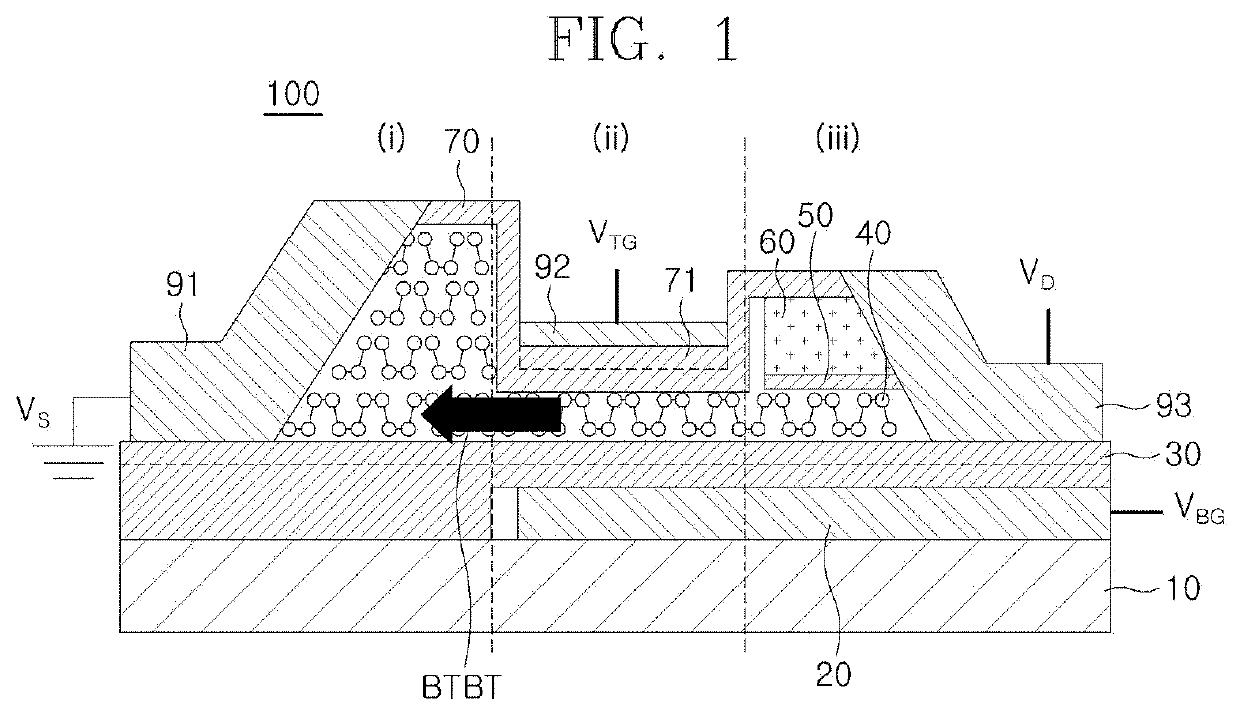
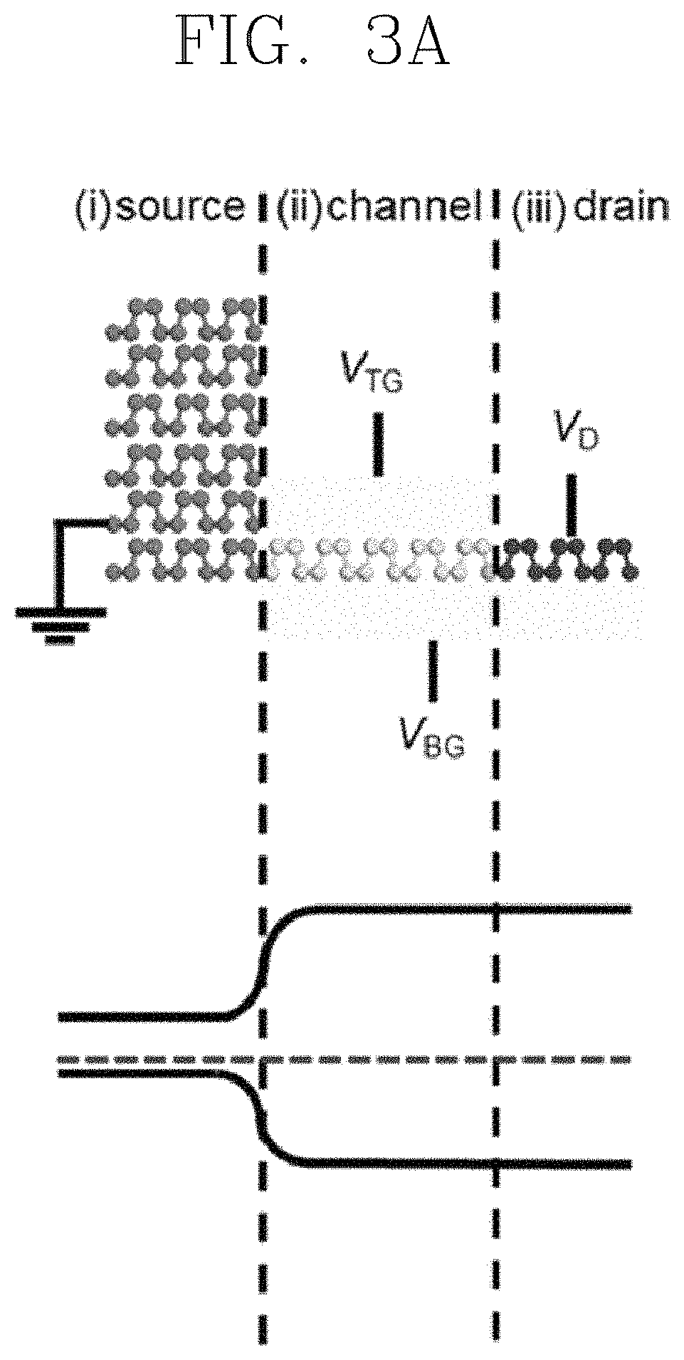
>[0030]The motive for arriving at the present disclosure and the theoretical background thereof will now be described in detail.

[0031]Conventional down scaling of transistors according to Moore's law has enabled today's information technology, but Moore's law is approaching its limit. That is, as described above, a conventional complementary metal-oxide semiconductor (CMOS) transistor needs at least 60 mV of switching voltage (subthreshold swing (SS) 60 mV / dec) each time the current increases ten times.

[0032]As an alternative thereto, TFETs are widely studies as a candidate group for accomplishing SS far lower than 60 mV / dec by means of high ON current I60 (current at which SS becomes 60 mV / dec), due to sub-thermionic SS.

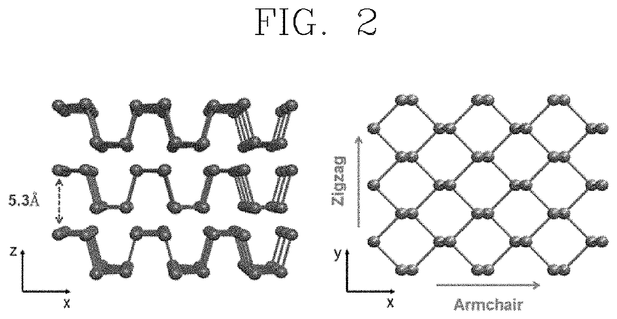
[0033]More specifically, it is theoretically predicted that HJ-TFETs will have high I60, and conventional research has failed to satisfy the theoretically expected value due to problems such as defects occurring at the heterojunction (HJ) interface made of heterogen...


PUM

PropertyMeasurementUnit
thicknessaaaaaaaaaa
switching voltageaaaaaaaaaa
thicknessaaaaaaaaaa

Abstract

Disclosed is a 2D-3D HJ-TFET made of a material, the band gap of which changes according to the thickness, such as black phosphorous or TMDC, in order to extend Moore's law. More particularly, disclosed are the structure of a 2D-3D HJ-TFET and a method for manufacturing the same, wherein the 2D-3D HJ-TFET is made of a material such as black phosphorous or TMDC such that the same consumes less power, has a high switching speed, can operate in a complementary manner so as to replace a conventional CMOS transistor, and can extend Moore's law.

Description

CROSS-REFERENCE TO RELATED APPLICATION[0001]This application claims priority to Korean Patent Application No. 10-2019-0086206 filed Jul. 17, 2019, the disclosure of which is hereby incorporated by reference in its entirety.BACKGROUND OF THE INVENTION1. Field of the Invention[0002]The present disclosure relates to a novel tunnel field-effect transistor (TFET) which consumes less power, which has a high switching speed, which can operate in a complementary manner so as to replace a complementary metal-oxide semiconductor (CMOS) transistor, and which is configured to extend Moore's law. More particularly, the present disclosure relates to the structure of a 2D-3D heterojunction tunnel field-effect transistor (HJ-TFET) employing a material, the band gap energy of which changes depending on the thickness thereof, such as black phosphorous or transition metal dichalcogenide (TMDC), and a method for manufacturing the same.2. Description of the Prior Art[0003]Due to power consumption limita...

Claims


Application Information

Patent Timeline
Patent Type & Authority Patents(United States)
IPC IPC(8): H01L29/76H01L29/24H01L29/45H01L29/66H01L29/786H01L29/18
CPCH01L29/7606H01L29/18H01L29/24H01L29/45H01L29/66969H01L29/66977H01L29/78648H01L29/78696H01L29/0847H01L29/1033H01L29/66356H01L29/7391B82Y10/00H01L29/0665H01L29/083H01L29/778H01L21/0228H01L21/02293H01L29/7786H01L2924/10325
Inventor CHO, SUNGJAE
Owner KOREA ADVANCED INST OF SCI & TECH
Why Eureka
Try Eureka