Method of forming a GaN sensor having a controlled and stable threshold voltage

a threshold voltage and sensor technology, applied in the field of algan/gan sensors, can solve the problems of complex sensor manufacturing, difficult control of the recess process uniformity, and increased device threshold voltage, so as to reduce current leakage, reduce the amount of dielectric material, and improve the thickness of the algan sensing region.

Active Publication Date: 2021-12-07
TOWER SEMICONDUCTOR
View PDF5 Cites 1 Cited by
  • Summary
  • Abstract
  • Description
  • Claims
  • Application Information

AI Technical Summary

Benefits of technology

[0013]In an alternate embodiment, the GaN hetero-structure additionally includes an etch stop layer formed over the first AlGaN barrier layer, and a second AlGaN barrier layer formed over the etch stop layer. In this alternate embodiment, etching the GaN heterostructure through the second mask includes performing an etch that removes portions of the second AlGaN barrier layer exposed through the second mask, wherein the etch is stopped on the etch stop layer. In this embodiment, the etch stop layer has a different composition than the first and second AlGaN barrier layers, allowing for etch selectivity. For example, the first and second AlGaN barrier layers may have a composition of AlxGayN, wherein 0<x and y<1, while the etch stop layer may have a composition of AlxGayN, wherein 0.5<x≤1, and 0≤y<0.5. In this embodiment, the initial fabricated thickness of the first AlGaN barrier layer remains in the final sensor structure, advantageously providing good control over the thickness of the AlGaN sensing region in the final sensor structure.
[0014]In one embodiment, the metal layer has an etch profile that is vertical with respect to the upper surface of the first AlGaN barrier layer, but the etch of the gate dielectric layer is controlled such that the gate dielectric layer has an etch profile that is sloped with respect to the upper surface of the first AlGaN barrier layer. As a result, the edges of the remaining gate dielectric regions are not vertical, but rather, are sloped at an acute angle with respect to the upper surface of the first AlGaN barrier layer. In a particular embodiment, this acute angle is greater than 20 degrees. In an alternate embodiment, this acute angle is less than 70 degrees. In yet another embodiment, this acute angle is greater than 70 degrees. These sloped edges of the remaining gate dielectric regions advantageously increase the distance (and the amount of dielectric material present) between the edges of the remaining metal structures and the exposed regions of the GaN hetero-structure. This advantageously reduces current leakage from the gate electrodes to the underlying 2DEG channel, thereby maintaining a stable transistor structure.
[0015]In one embodiment, dielectric spacers are formed on the sidewalls of the remaining metal structures, as well as the sidewalls of the gate dielectric regions. These dielectric spacers extend from the sidewalls of the remaining metal structures (i.e., source contact, drain contact and gate electrodes) to the GaN heterostructure (e.g., the first AlGaN barrier layer or the etch stop layer). As a result, these dielectric spacers advantageously increase the distance (and the amount of dielectric material present) between the edges of the remaining metal structures and the exposed regions of the GaN heterostructure. Again, this advantageously reduces current leakage from the gate electrodes to the underlying 2DEG channel, thereby maintaining a stable transistor structure.
[0016]In accordance with another embodiment, the back side surface of the substrate is etched, thereby defining a membrane region of the sensor. The back side of the substrate is etched by: (1) forming a mask over the back side of the substrate, wherein the mask includes an opening that defines the membrane region of the sensor, (2) performing a dry etch through the opening of the mask, wherein the dry etch extends only partially through the substrate; and then, (3) performing a wet etch through the opening of the mask, wherein the wet etch extends entirely through the substrate. This wet etch advantageously avoids plasma damage to structures fabricated at the front side of the sensor, including the gate dielectric structures.
[0018]In another embodiment, a functionalization layer is formed on the exposed region of the GaN heterostructure, wherein the functionalization layer aids in the detection of an external influence.

Problems solved by technology

However, one of the main challenges in the formation of sensors that implement MIS gate structures is the realization of a controlled and stable system such that changes in device threshold voltage (Vt) are related only to external influences and not to non-uniformities of the manufacturing process.
Three components of the manufacturing process may result in non-uniformities.
However, a main obstacle of this technique is difficulty in controlling the recess process uniformity, and consequently, the device threshold voltage.
This concept undesirably requires additional steps of tungsten deposition, lithography and etch, which make sensor manufacturing more complex.
The disadvantage of this approach is process control.

Method used


Image

  • Method of forming a GaN sensor having a controlled and stable threshold voltage
  • Method of forming a GaN sensor having a controlled and stable threshold voltage
  • Method of forming a GaN sensor having a controlled and stable threshold voltage

Examples


Embodiment Construction

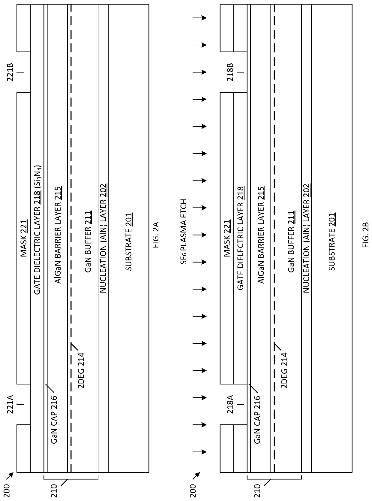
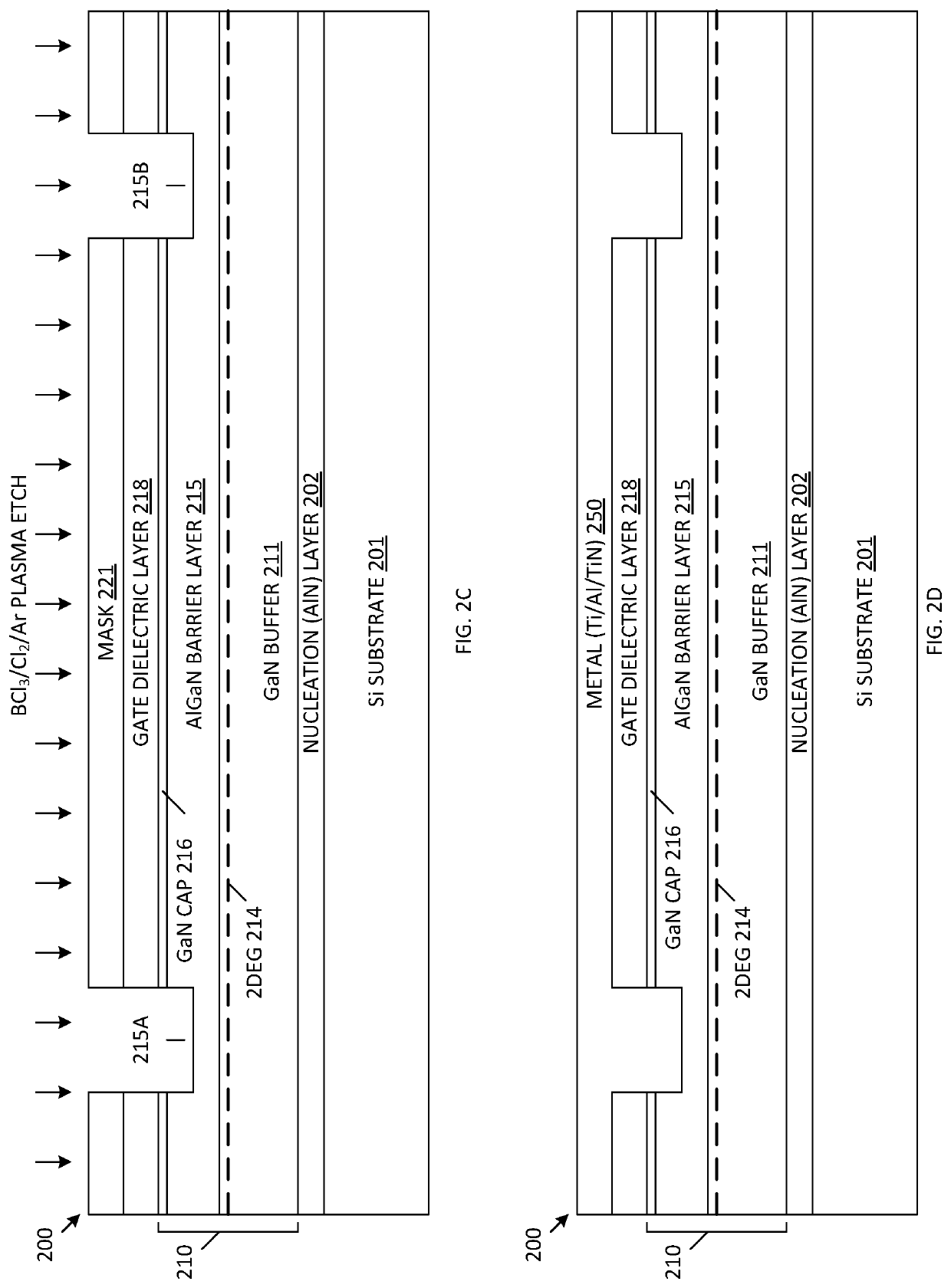
6]FIGS. 2A-2K are cross sectional views of a GaN sensor 200 that includes a gate dielectric having a sloped profile during various processing steps in accordance with an one embodiment of the present invention. As illustrated by FIG. 2A, sensor 200 is fabricated on a substrate 201. In the described embodiments, substrate 201 is high resistance monocrystalline silicon (having a crystal orientation), advantageously reducing the costs associated with fabricating sensor 200. However, in other embodiments, substrate 201 can be sapphire, silicon carbide (SiC), or a flexible material. Nucleation layer 202 is formed on the upper surface of substrate 201. In the described embodiments, nucleation layer 202 is aluminum nitride (AlN). The nucleation layer 202 is selected to compensate for the mismatch of lattice constants between the substrate 201 and the subsequently formed gallium nitride (GaN) buffer 211. GaN buffer 211 includes one or more GaN layers, which may be interleaved with one or m...


PUM

PropertyMeasurementUnit
thicknessaaaaaaaaaa
thicknessaaaaaaaaaa
acute angleaaaaaaaaaa

Abstract

A method fabricating a GaN based sensor including: forming a gate dielectric layer over a GaN hetero-structure including a GaN layer formed over a substrate and a first barrier layer formed over the GaN layer; forming a first mask over the gate dielectric layer; etching the gate dielectric layer and the first barrier layer through the first mask, thereby forming source and drain contact openings; removing the first mask; forming a metal layer over the gate dielectric layer, wherein the metal layer extends into the source and drain contact openings; forming a second mask over the metal layer; etching the metal layer, the gate dielectric layer and the GaN heterostructure through the second mask, wherein a region of the GaN heterostructure is exposed; and thermally activating the metal layer in the source and drain contact openings. The gate dielectric may exhibit a sloped profile, and dielectric spacers may be formed.

Description

FIELD OF THE INVENTION[0001]The present invention relates to an AlGaN / GaN sensor having a metal-insulator-semiconductor (MIS) high electron-mobility transistor (HEMT) structure with improved isolation between the gate and AlGaN open surface regions, thereby providing a stable device with threshold voltage (Vt) control of the sensing area.RELATED ART[0002]AlGaN / GaN high electron mobility transistors (HEMTs) are currently primarily used for power management and radio frequency (RF) applications, which benefit from high breakdown fields and high two-dimensional electron gas (2DEG) mobility provided by GaN transistors. There is growing interest in the use of such HEMT hetero-structures for sensing applications due to the robustness of this material system in extreme conditions (pressure, temperature, corrosive, radiation), especially when compared to conventional silicon-based devices. There are numerous examples of sensing applications that use 2DEG resistance changes in simple systems...

Claims


Application Information

Patent Timeline
Patent Type & Authority Patents(United States)
IPC IPC(8): H01L29/66H01L21/8234H01L29/205H01L29/20H01L29/40H01L29/417
CPCH01L29/66462H01L21/823462H01L29/2003H01L29/205H01L29/401H01L29/41766H01L29/7786H01L29/0657H01L29/42368H01L21/31116H01L21/30621H01L21/30617G01N27/4141H01L29/7787
Inventor SHIMA-EDELSTEIN, RUTHSHAUL, RONENSTRUL, ROYSERGIENKO, ANATOLYPOLIAK, LIZGILAD, IDOSIRKIS, ALEXROIZIN, YAKOV
Owner TOWER SEMICONDUCTOR
Why Eureka
Try Eureka