
Eureka
For R&D, Eureka makes reading and utilizing patents & technical documents easy.
Eureka AIR
Designed for self-driven R&D workflows. Generate viable solutions, solve complex R&D challenges, empower your innovation with AI.

Eureka Materials
Designed for material experts only. Revolutionize your material R&D, from search, analyze, to developing new materials.

TechResearch
Generate reliable direction feasibility study reports for your R&D in just a few steps.

TechSeek
Discover and master advanced knowledge NOW. Basics, ideas, possibilities, all at once.

TechMind
As an expert in R&D Theories, TechMind can generates customized viable solutions instantly.

TechRisk
Analyze your overall solution with one click, know your potential R&D risks in advance.

TechMonitor
Get weekly tech updates, stay abreast of the latest tech innovations and key insights.
Trench planar MOS cell for transistors
- Summary
- Abstract
- Description
- Claims
- Application Information
AI Technical Summary
Benefits of technology
Problems solved by technology
Method used
Image

Examples
first embodiment
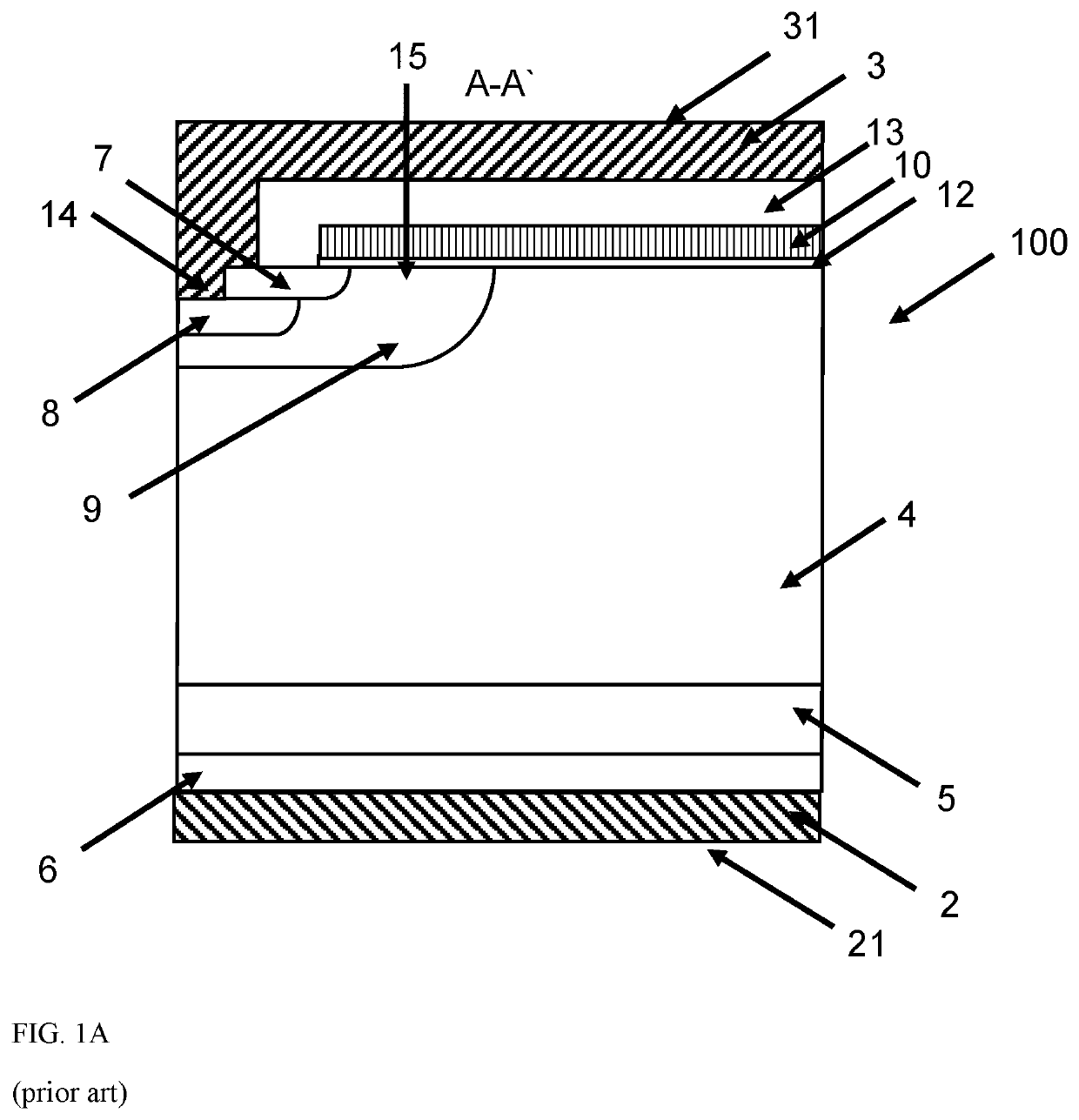
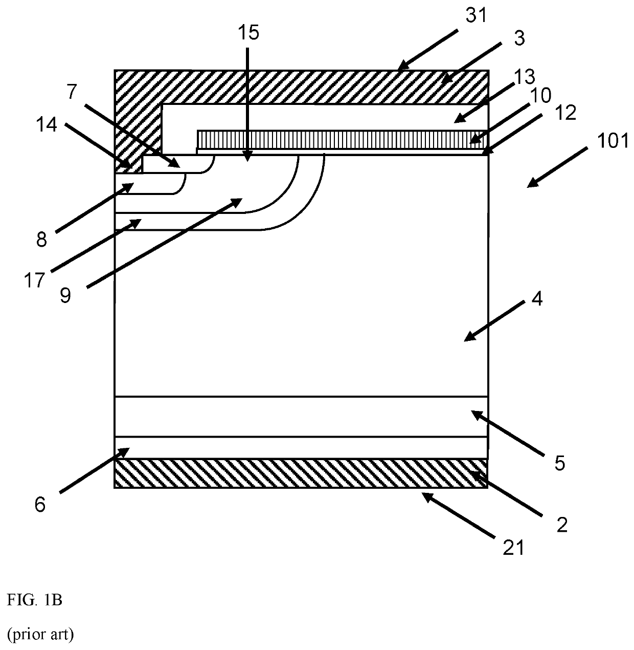
[0053]The polygon configurations of the transistor cell regions are best shown in FIG. 7A, which is first described. Referring to this figure, the top plane view of the transistor cell shows only the critical layers, and is depicting a manufacturing stage prior to the application of the dielectric layer (13) and of the emitter electrode layer (3). The transistor cell layout is depicted as a square shape in FIG. 7A, but can have any other polygonal shape such as hexagons, rectangles. triangles or even rounded shapes. Additionally, FIG. 7A depicts two second gate electrodes (11) formed in trench recesses, and a polygonal opening in the first planar gate electrode layer (10) that overlays a plurality of source regions (7) with contact openings (14), all these layers being formed on the emitter side (31) of the transistor. The two trench recesses are arranged orthogonal to each other, each of them parallel to one of the two main sides of the square cell. Other regular and irregular sha...
seventh embodiment
[0067]A seventh embodiment is shown in FIG. 14A, wherein the first base layer (9) extends uniformly on the top of, and substantially overlaps the drift layer (4) in the regions under the first planar gate electrode (10). In this case, although an inversion layer can be formable in the first base layer (9) regions under the first gate electrode (10), a planar MOS channel (15) is not formable in the traditional understanding, as the drift layer (4) is not directly connected to this inversion layer on the emitter side. Instead, the majority charge carriers will flow on the side trench walls of the second gate electrodes (11) as depicted in FIG. 14B.
eighth embodiment
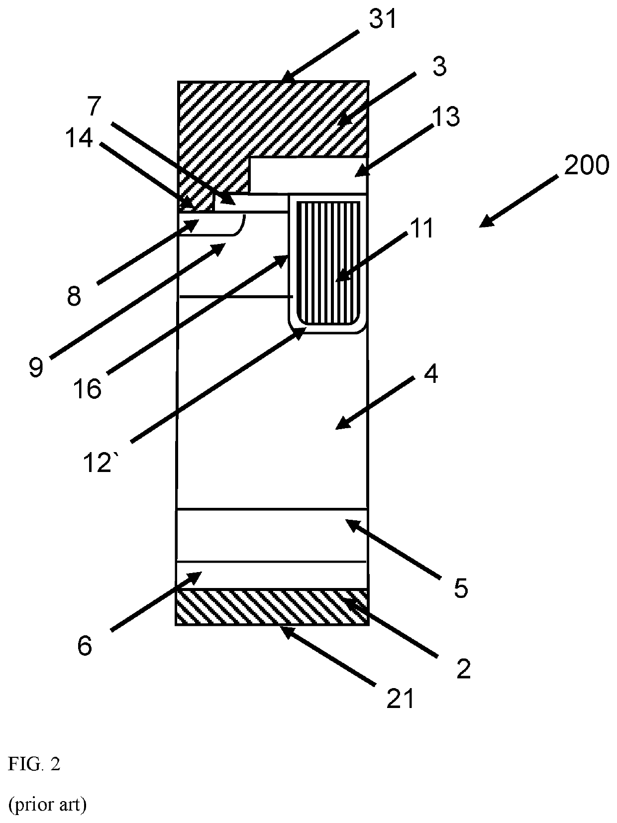
[0068]In an eighth embodiment, shown in FIG. 15 as a cross section through the transistor cell, the second base layer (8) may be laterally extending to abut the insulating layer (12′). In this case, as the P type doping of the second base layer (8) is higher than the P type doping of the first base layer (9), a vertical MOS channel (16) is not formable when a voltage is applied on the second gate electrode (12′), while the same voltage applied on the first gate electrode (10) will still form a planar MOS channel (15).
[0069]In all the embodiments described above, the trench recesses embedding the second gate electrodes (11), will extend vertically into the drift layer (4) to a depth approximately in a range from about 2 μm to about 10 μm. Additionally, the width of the trenches may range from about 3 μm to about 0.5 μm. Alternatively, it may also be possible that the trench recesses embedding the second gate electrodes (11) are etched shallower than the depth of the first base layer ...
PUM
 Abstract
Description
Claims
Application Information
 - R&D Engineer
- R&D Manager
- IP Professional
- Industry Leading Data Capabilities
- Powerful AI technology
- Patent DNA Extraction
Browse by: Latest US Patents, China's latest patents, Technical Efficacy Thesaurus, Application Domain, Technology Topic, Popular Technical Reports.
© 2024 PatSnap. All rights reserved.Legal|Privacy policy|Modern Slavery Act Transparency Statement|Sitemap|About US| Contact US: help@patsnap.com