Switch device, storage apparatus, and memory system incorporating boron and carbon

a technology of boron and carbon, which is applied in the direction of digital storage, semiconductor devices, instruments, etc., can solve the problems of difficult increase in capacity and large floor area per unit cell, and achieve the effects of increasing capacity, small floor area and increasing capacity

Active Publication Date: 2022-10-04
SONY SEMICON SOLUTIONS CORP
View PDF14 Cites 1 Cited by
  • Summary
  • Abstract
  • Description
  • Claims
  • Application Information

AI Technical Summary

Benefits of technology

[0011]It is desirable to provide a switch device that makes it possible to improve heat resistance, and a storage apparatus and a memory system that each include the switch device.
[0015]In the switch device according to the embodiment of the present disclosure, the storage apparatus according to the embodiment of the present disclosure, and the memory system according to the embodiment of the present disclosure, the switch layer includes selenium (Se), at least one kind of germanium (Ge) or silicon (Si), boron (B), carbon (C), gallium (Ga), and arsenic (As). This makes it possible to reduce alteration of the switch layer caused by a heat load in a manufacturing process.
[0016]According to the switch device according to the embodiment of the present disclosure, the storage apparatus according to the embodiment of the present disclosure, and the memory system according to the embodiment of the present disclosure, the switch layer is formed using selenium (Se), at least one kind of germanium (Ge) or silicon (Si), boron (B), carbon (C), gallium (Ga), and arsenic (As), which reduces alteration of the switch layer caused by the heat load in the manufacturing process. This makes it possible to improve heat resistance of the switch device using selenium (Se).

Problems solved by technology

In existing resistance change memories each using an access transistor, however, a floor area per unit cell is large.
Therefore, the increase in capacity is not easy even if miniaturization is performed under the same design rule, as compared with, for example, flash memories such as an NAND flash memory.

Method used


Image

  • Switch device, storage apparatus, and memory system incorporating boron and carbon
  • Switch device, storage apparatus, and memory system incorporating boron and carbon
  • Switch device, storage apparatus, and memory system incorporating boron and carbon

Examples


embodiment

1. Embodiment

(An example in which a switch layer includes selenium (Se), at least one kind of germanium (Ge) or silicon (Si), boron (B), carbon (C), gallium (Ga), and arsenic (As))

[0039]1-1. Configuration of Switch Device

[0040]1-2. Configuration of Memory Cell Array

[0041]1-3. Workings and Effects

2. Modification Examples

[0042]2-1. Modification Example 1 (Another example of a memory cell array having a planar configuration)

[0043]2-2. Modification Example 2 (An example of a memory cell array having a three-dimensional configuration)

3. Application Example (Data storage system)

4. Examples

first embodiment

1. First Embodiment

1-1. Configuration of Switch Device

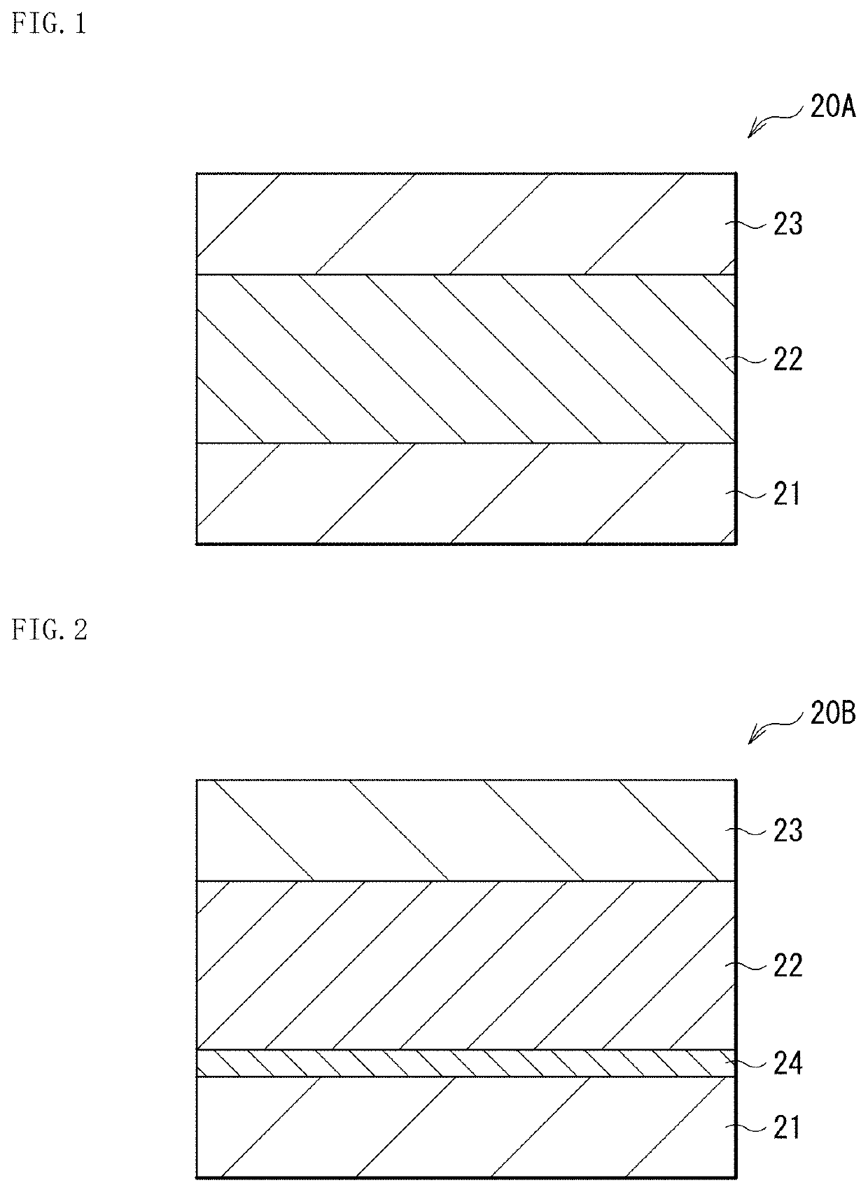
[0044]FIG. 1 illustrates an example of a cross-sectional configuration of a switch device (a switch device 20A) according to an embodiment of the present disclosure. The switch device 20A selectively operates any of a plurality of storage devices (memory devices 30; FIG. 5) arranged in a memory cell array 1 having a so-called cross point array structure illustrated in FIG. 5, for example. The switch device 20A (a switch device 20; FIG. 5) is coupled in series to the memory device 30 (specifically, a memory layer 31), and includes a lower electrode 21 (a first elect a switch layer 22, and an upper electrode 23 (a second electrode) in this order.

[0045]The lower electrode 21 includes a wiring material used for a semiconductor process. Examples of the wiring material include tungsten (W), tungsten nitride (WN), titanium nitride (TiN), copper (Cu), aluminum (Al), molybdenum (Mo), tantalum (Ta), tantalum nitride (TaN), silicide, and th...

modification examples

2. Modification Examples

2-1. Modification Example 1

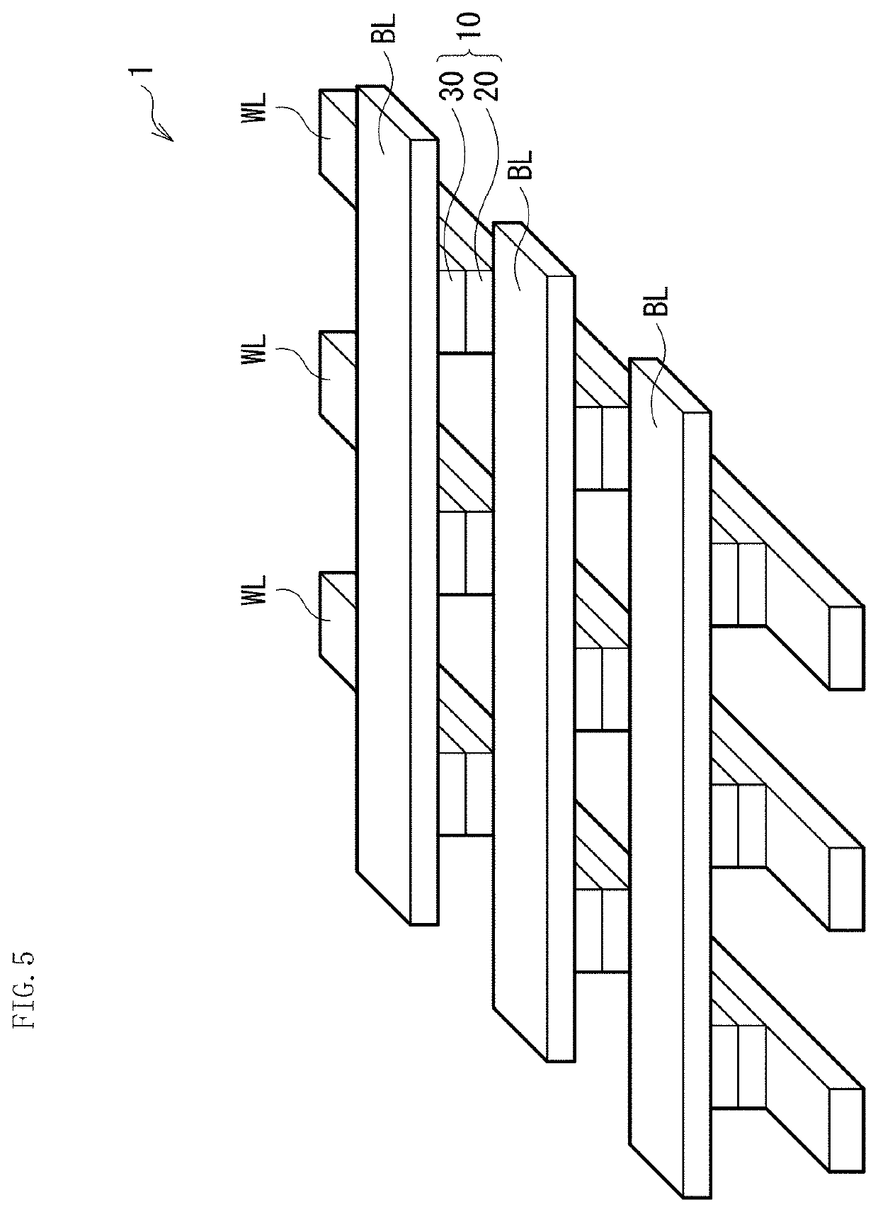
[0087]FIG. 9 illustrates an example of a configuration of a memory cell array 2 according to a modification example of the present disclosure in perspective view. The memory cell array 2 has a so-called cross point array structure, as with the memory cell array 1 described above. In the present modification example, the memory device 30 includes the memory layer 31 extending along each of the bit lines BL that extend in directions common to each other. The switch device 20 includes the switch layer 22 extending along each of the word lines WL that extend in a direction different from the extending directions of the bit lines BL (for example, in a direction orthogonal to the extending directions of the bit lines BL). The switch layer 22 and the memory layer 31 are stacked with the intermediate electrode 41 interposed therebetween at cross points of the plurality of word lines WL and the plurality of bit lines BL.

[0088]As described ab...


PUM

PropertyMeasurementUnit
thicknessaaaaaaaaaa
thicknessaaaaaaaaaa
thicknessaaaaaaaaaa

Abstract

A switch device according to an embodiment of the present disclosure includes a first electrode; a second electrode opposed to the first electrode; and a switch layer including selenium (Se), at least one kind of germanium (Ge) or silicon (Si), boron (B), carbon (C), (Ga), and arsenic (As), and provided between the first electrode and the second electrode.

Description

CROSS REFERENCE TO RELATED APPLICATIONS[0001]This application is a national stage application under 35 U.S.C. 371 and claims the benefit of PCT Application No. PCT / JP2019 / 0003426 having an international filing date of 31 Jan. 2019, which designated the United States, which PCT application claimed the benefit of Japanese Patent Application No. 2018-037817 filed 2 Mar. 2018, the entire disclosures of each of which are incorporated herein by reference.TECHNICAL FIELD[0002]The present disclosure relates to a switch device including a chalcogenide layer between electrodes, and to a storage apparatus and a memory system that each include the switch device.BACKGROUND ART[0003]In recent years, an increase in capacity is demanded for data storage non-volatile memories represented by resistance change memories such as a ReRAM (resistance random access memory) and a PRAM (Phase-Change Random Access Memory) (registered trademark). In existing resistance change memories each using an access tran...

Claims


Application Information

Patent Timeline
Patent Type & Authority Patents(United States)
IPC IPC(8): H01L45/00G11C13/00H01L27/22H01L27/24
CPCH01L45/143G11C13/0004H01L45/085G11C13/0069G11C2213/70H01L27/224H01L27/249H01L27/2427H01L27/2463H01L45/145G11C13/003G11C2213/76G11C2213/52G11C13/0007G11C11/1659G11C2213/15G11C2213/71H10B63/24H10B63/80H10B63/845H10N70/231H10N70/8825H10B61/00H10B63/00H10N70/8845H10B61/10H10N70/245H10N70/883
Inventor SEI, HIROAKIOHBA, KAZUHIROYASUDA, SHUICHIRO
Owner SONY SEMICON SOLUTIONS CORP
Why Eureka
Try Eureka