Method of detecting and measuring endpoint of polishing processing and its apparatus and method of manufacturing semiconductor device using the same

a technology of polishing processing and endpoint detection, which is applied in the direction of lapping machines, instruments, abrasive surface conditioning devices, etc., can solve the problems of reducing the polishing performance of pad 1, the insulating film layer on the wafer surface has flaws, and the polishing performance of pad 1 is difficult to achieve uniform exposure conditions, etc., to achieve high-precision film thickness, increase the accuracy and improve the effect of detecting the endpoin

Inactive Publication Date: 2002-09-12
HITACHI LTD
View PDF2 Cites 73 Cited by
  • Summary
  • Abstract
  • Description
  • Claims
  • Application Information

AI Technical Summary

Benefits of technology

0016] In other words, in accordance with a first aspect of the present invention, there is provided a method and an apparatus for detecting an endpoint of polishing processing, wherein the film formed on a wafer surface under polishing processing is irradiated with lights having two or more different wavelengths, a white light or an ultraviolet (UV) light, and a film thickness of the film formed on the semiconductor device surface is evaluated based on an intensity of a reflected light or a spectral intensity from the film or an intensity of the UV light, thereby detecting an endpoint of polishing processing for the film. According to these method and apparatus, it is possible to increase an accuracy of detecting the endpoint of polishing processing for the film even for a small polishing processing amount or independently of a film structure.
0017] In a second aspect of the present invention, there is provided a polishing processing method with an endpoint detection function and its apparatus, wherein the film formed on a wafer surface under polishing processing is irradiated with lights having two or more different wavelengths, a white light or an ultraviolet (UV) light, and a film thickness of the film formed on the semiconductor device surface is evaluated based on an intensity of a reflected light or a spectral intensity from the film or an intensity of the UV light, thereby detecting an endpoint of polishing processing for the film to terminate the polishing processing. According to these method and apparatus, it is possible to increase an accuracy of detecting the endpoint of polishing processing for the film even for a small polishing processing amount or independently of a film structure.
0018] In accordance with a third aspect of the present invention, there is provided a method of manufacturing a semiconductor device, wherein means for evaluating the film thickness is incorporated into a polishing processing machine to evaluate a deteriorated condition of a polishing pad, thereby optimizing the polishing processing conditions and dressing conditions of the pad at the polishing processing. With this method, an object to be polished, for example, a film formed on the wafer becomes further smoother, thus enabling a high-precision film thickness control or a high-grade polishing processing control to improve a throughput.
0019] The semiconductor device manufacturing method according to the present invention may be such that the condition is evaluated at a plurality of positions on the wafer surface by pad evaluation means, thereby enabling an evaluation of a film thickness distribution of a wafer and a film on the wafer surface during processing.
0020] In addition the semiconductor device manufacturing method according to the present invention may be such that a CMP process can be stabilized and optimized on the basis of a film evaluation result of the film formed on the wafer surface.

Problems solved by technology

The under element or wiring pattern, however, generates an uneven surface of the layer insulating film provided to form the next layer on the element or wiring pattern layer on the wafer.
The increase of the unevenness on the surface of the layer insulating film makes it hard to achieve a uniform exposure condition over the entire film formed on the layer insulating film, and therefore the layer insulating film is smoothed before forming the film.
If a lot of wafers are polished, however, the pad 1 wears out on its surface, thereby decreasing a polishing performance of the pad 1 or causing a serious condition in which the layer insulating film on the wafer surface has flaws due to contaminants adhering to the surface of the pad 1.
As an important problem in this CMP processing, there is an endpoint detection for terminating polishing when the layer insulating film on the wafer surface has been polished into a predetermined film thickness.
In these methods, however, the detection cannot be precisely controlled due to uneven polishing rates and further the control takes plenty of time.
Therefore, a gradient of the curve P is low and therefore even if a predetermined intensity I is detected, it is hard to detect it accurately.
Accordingly the conventional in-situ measurement is effective for a relatively large processing amount (polishing amount), while it is often incapable of detecting an endpoint accurately in case of a small processing amount or according to a film structure.

Method used


Image

  • Method of detecting and measuring endpoint of polishing processing and its apparatus and method of manufacturing semiconductor device using the same
  • Method of detecting and measuring endpoint of polishing processing and its apparatus and method of manufacturing semiconductor device using the same
  • Method of detecting and measuring endpoint of polishing processing and its apparatus and method of manufacturing semiconductor device using the same

Examples


first embodiment

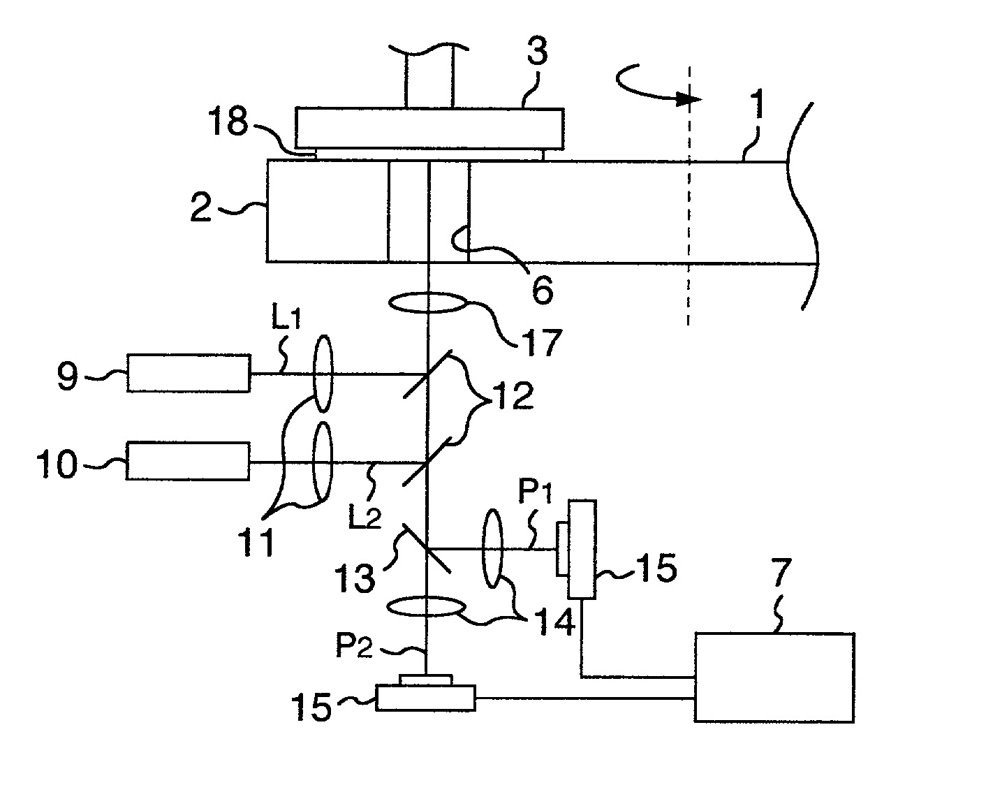
[0045] Referring to FIG. 1, there is shown a constitutional diagram of a main portion of a method and an apparatus for detecting an endpoint of polishing processing according to the present invention, including laser light sources 9 and 10, a lens 11, a beam splitter 12, a dichroic mirror 13, a lens 14, optical detectors 15 and 16, an objective lens 17, and a wafer 18, where identical reference numerals are used for the portions corresponding to those in FIG. 20 to omit overlapped descriptions.

[0046] In this figure, the laser light sources 9 and 10 emits laser lights L.sub.1 and L.sub.2 having different wavelengths. These laser lights L.sub.1 and L.sub.2 are changed to beams by the lens 11, reflected on the beam splitter 12, and then emitted to the wafer 18 held by a wafer chuck via the objective lens 17 and the detection window 6 provided penetrating the polishing disk 2 and the pad 1 from the side of a layer insulating film (not shown). In this condition, the laser lights L.sub.1 ...

second embodiment

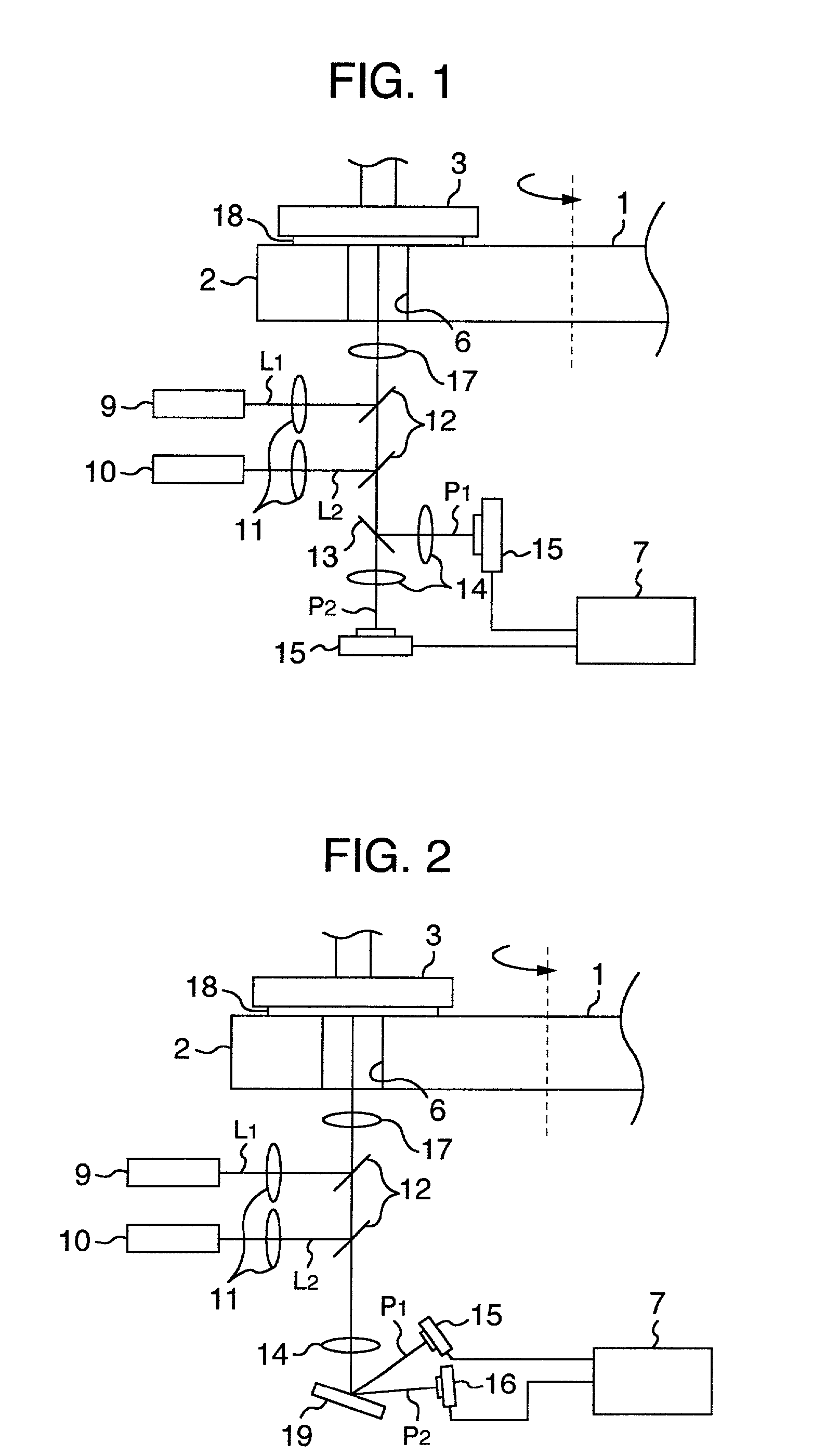
[0049] While the interference lights P.sub.1 and P.sub.1 caused by the laser lights L.sub.1 and L.sub.2 having different wavelengths are separated by using the dichroic mirror 13 in the embodiment shown in FIG. 1, they can be separated by using a diffraction grating 19 as shown in FIG. 2 as a Furthermore, it is also possible to use other wavelength separating means such as a prism other than the above.

[0050] Furthermore, as the optical detectors 15 and 16 in FIG. 1 and FIG. 2, it is possible to use a CCD two-dimensional sensor or one-dimensional line sensor or other optical sensors other than the CCD sensors.

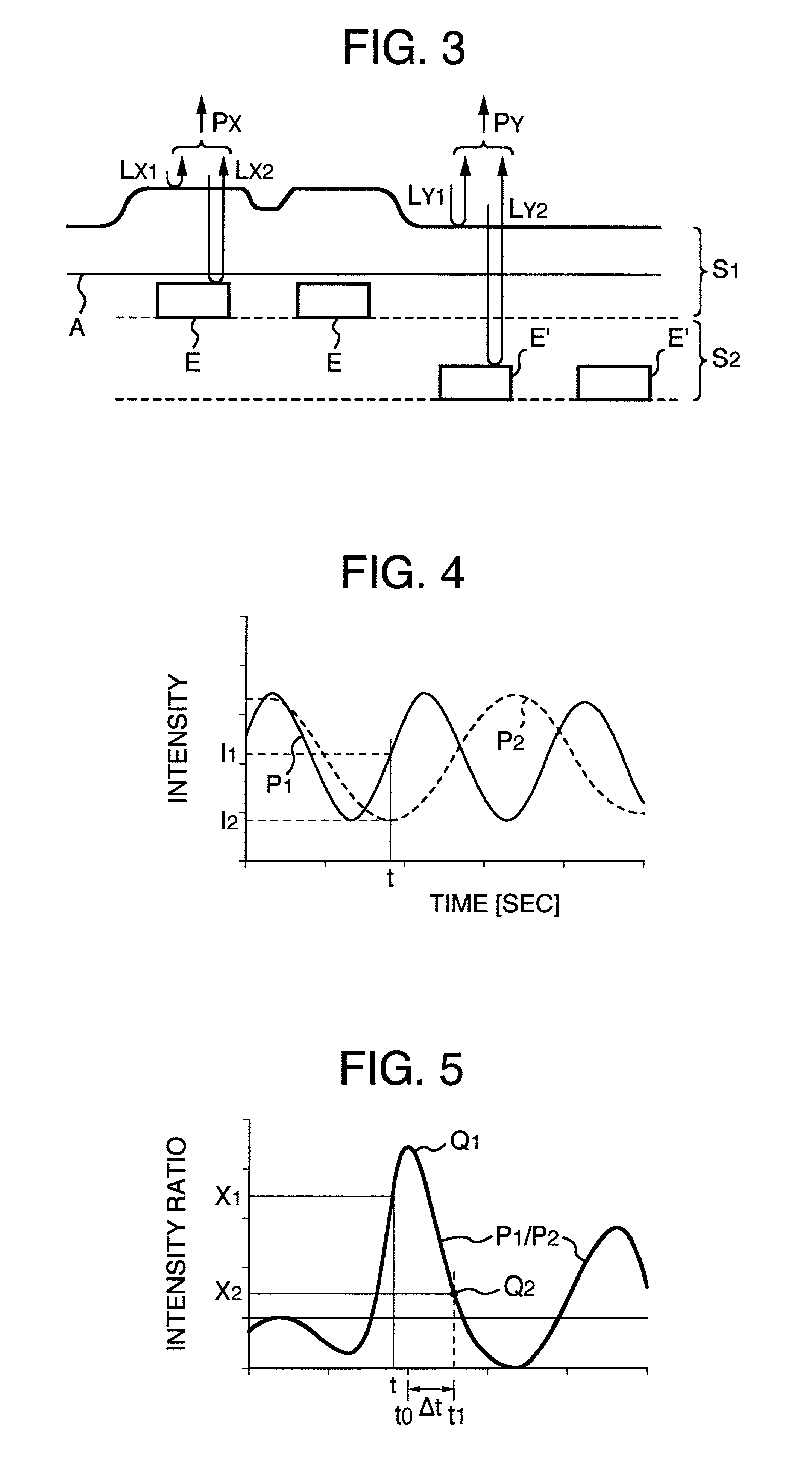
[0051] If the single detection window 6 is provided on the polishing disk 2 and the wafer 18 is located on an extension line of the optical axis of the objective lens 17 in FIG. 1 and FIG. 2, the optical detectors 15 and 16 detect the interference lights P.sub.1 and P.sub.2 intermittently once per rotation of the polishing disk 2. These interference lights P.sub.1 and P.sub.2 a...

third embodiment

[0076] Referring to FIG. 7, there is shown a constitutional diagram of a main portion of a method and an apparatus for detecting an endpoint of polishing processing according to the present invention, including a white light source 20 and a spectrograph 21, with components corresponding to those in the above drawings designated by identical reference numerals to omit overlapped descriptions.

[0077] In this third embodiment, a white light source is used for a light source.

[0078] In FIG. 7, the white light source 20 emits a white light L. The white light L is changed to beams by a lens 11, reflected on a beam splitter 12, and then emitted to the wafer 18 via an objective lens 17 and a detection window 6 from the side of a layer insulating film (not shown). In this embodiment in the same manner as for the above embodiments, the white light L causes an interference for each wavelength component between a reflected light from a surface of the layer insulating film and a reflected light fr...


PUM


Abstract

Laser sources output laser lights L.sub.1 and L.sub.2 having different wavelengths so as to increase an accuracy of an endpoint detection of polishing processing by enabling an accurate detection of a film thickness of a layer insulating film on a surface of a wafer to be polished by the CMP processing, the lights are emitted from a detection window via a beam splitter to the layer insulating film formed on the surface of the wafer to be polished by a pad, different optical detectors detect interference lights corresponding to the laser lights L.sub.1 and L.sub.2 reflected and generated from a surface of the layer insulating film and a pattern under the surface via the detection window, the beam splitter, and a dichroic mirror, the detection results are supplied to a film thickness evaluation unit 7, a film thickness of the layer insulation film is detected on the basis of a relationship between intensities of the reflected interference lights to the laser lights L.sub.1 and L.sub.2 or the intensity ratio, and an endpoint of polishing processing is determined when the film thickness is equal to a predetermined value.

Description

BACKGROUND OF THE INVENTION[0001] 1. Field of the Invention[0002] The present invention relates to an endpoint detecting of polishing processing of a semiconductor device, and more particularly to a method of detecting an endpoint in smoothing of a wafer surface and its apparatus, a polishing method with an endpoint detecting function and its apparatus, and a method of manufacturing a semiconductor device using the same.[0003] 2. Related Background Art[0004] A semiconductor device is manufactured by forming a film on a silicon wafer (hereinafter simply referred to as wafer) and forming an element or wiring pattern through an exposure in a desired pattern and an etching process of the exposed portion. Subsequently to forming the element or wiring pattern as described above, a transparent layer insulating film made of SiO.sub.2 or the like is formed to cover the element or wiring pattern and the next element or wiring pattern is formed on the layer insulating film, thus causing the ma...

Claims


Application Information

Patent Timeline
Patent Type & Authority Applications(United States)
IPC IPC(8): B24B37/013B24B53/00B24B49/04B24B49/12B24B53/017H01L21/304H01L21/306
CPCB24B37/013B24B49/04B24B49/12
Inventor HIROSE, TAKENORINOMOTO, MINEOKOJIMA, HIROYUKISATO, HIDEMI
Owner HITACHI LTD
Why Eureka
Try Eureka