Semiconductor laser device

a laser device and semiconductor technology, applied in semiconductor lasers, laser optical resonator construction, laser details, etc., can solve the problems of deteriorating window structure reproducibility, difficult to obtain high reliability, and difficult to obtain a highly reliable semiconductor laser at high yield

Inactive Publication Date: 2002-10-10
FUJIFILM HLDG CORP +1
View PDF0 Cites 13 Cited by
  • Summary
  • Abstract
  • Description
  • Claims
  • Application Information

AI Technical Summary

Problems solved by technology

In a semiconductor laser device, a current density at its edge facets increases under high power oscillation, so that an optical density increases and breakage and the like occurs at the edge facets, thereby making it difficult to obtain high reliability.
However, the window structure described above has a problem such that variations of thermal diffusion in a regrowth process make the depth of diffusion and the mixed crystallization uneven, deteriorati...

Method used


Image

  • Semiconductor laser device
  • Semiconductor laser device
  • Semiconductor laser device

Examples


Embodiment Construction

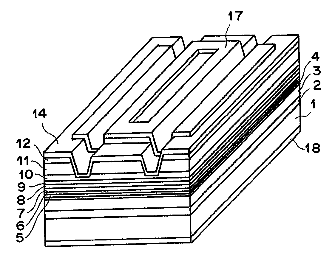
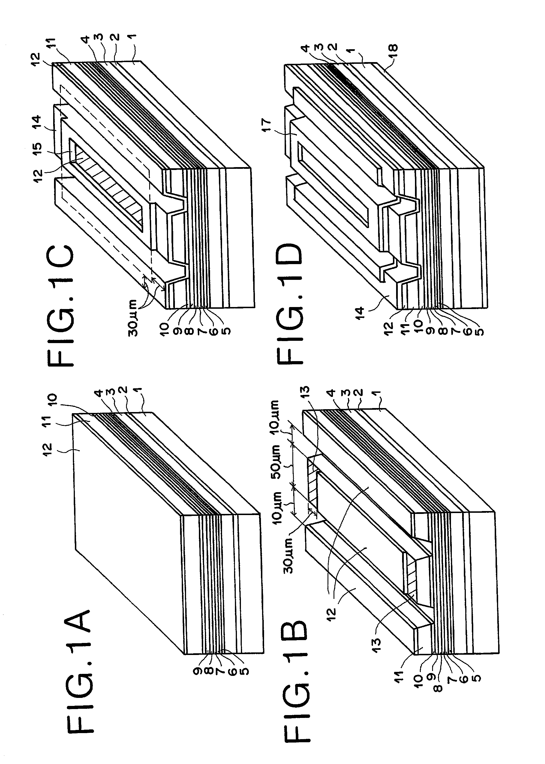
[0020] Description will be given of a semiconductor laser device according to an embodiment of the present invention, along its manufacturing process. FIGS. 1A to 1D are perspective views showing respective steps of fabricating the semiconductor laser device.

[0021] As shown in FIG. 1A, on a plane (100) of an n-type GaAs substrate 1, grown by organometallic vapor phase expitaxy are an n-type GaAs buffer layer 2, an n-type In.sub.0.48Ga.sub.0.52P lower cladding layer 3, an n-type or i-type In.sub.x1Ga.sub.1-x1As.sub.1-y1P.sub.y1 optical waveguide layer 4, an i-type GaAs.sub.1-y2P.sub.y2 tensile-strain barrier layer 5, an In.sub.x3Ga.sub.1-x3As.sub.1-y3P.sub.y3 compressive-strain quantum-well active layer 6, an i-type GaAs.sub.1-y2P.sub.y2 tensile-strain barrier layer 7, a p-type or i-type In.sub.x1Ga.sub.1-x1As.sub.1-y1P.sub.y1 upper optical waveguide layer 8, a p-type In.sub.0.48Ga.sub.0.52P first upper cladding layer 9, a GaAs etching stop layer 10, a p-type In.sub.0.48Ga.sub.0.52P ...


PUM


Abstract

A semiconductor laser device is disclosed that improves reliability during high-power oscillation. On a plane of an n-type GaAs substrate, grown are an n-type GaAs buffer layer, an n-type In0.48Ga0.52P lower cladding layer, an n-type or i-type Inx1Ga1-x1As1-y1Py1 optical waveguide layer, an i-type GaAs1-y2Py2 tensile-strain barrier layer, an Inx3Ga1-x3As1-y3Py3 compressive-strain quantum-well active layer, an i-type GaAs1-y2Py2 tensile-strain barrier layer, a p-type or i-type Inx1Ga1-x1As1-y1Py1 upper optical waveguide layer, a p-type In0.48Ga0.52P first upper cladding layer, a GaAs etching stop layer, a p-type In0.48Ga0.52P second upper cladding layer and a p-type GaAs contact layer. Two ridge trenches are formed on the resultant structure, and current non-injection regions are formed by removing the p-type GaAs contact layer in portions extending inwardly by 30 mum from cleavage positions of edge facets of the resonator on a top face of a ridge portion between the ridge trenches.

Description

[0001] 1. Field of the Invention[0002] The present invention relates to a semiconductor laser device, and particularly to a semiconductor laser device having a window structure formed therein.[0003] 2. Description of the Related Art[0004] In a semiconductor laser device, a current density at its edge facets increases under high power oscillation, so that an optical density increases and breakage and the like occurs at the edge facets, thereby making it difficult to obtain high reliability. Thus, there have been made many proposals concerning a structure, so-called a window structure, for providing current non-injection regions in the vicinities of the edge facets of a resonator.[0005] In the gazette of Japanese Unexamined Patent Publication No. 2000-31596 is, for example, a window structure fabricated in such a manner that a cladding layer disclosed is etched to the vicinity of a quantum-well active layer and a re-grown cladding layer added with dopant is formed, whereby the dopant ...

Claims


Application Information

Patent Timeline
IPC IPC(8): H01S5/16H01S5/223H01S5/34H01S5/343
CPCB82Y20/00H01S5/34386H01S5/3413H01S5/16
Inventor KUNIYASU, TOSHIAKIFUKUNAGA, TOSHIAKI
Owner FUJIFILM HLDG CORP
Why Eureka
Try Eureka