Pb-free solder-connected structure and electronic device

a technology of electronic devices and solder connections, applied in the direction of final product manufacturing, sustainable manufacturing/processing, and semiconductor/solid-state device details, etc., can solve the problems of pollution of the global environment by electrical appliances, and the effect of living things, ensuring the resistance to whisker formation, and ensuring the bonding strength

Inactive Publication Date: 2002-11-07
RENESAS ELECTRONICS CORP
View PDF8 Cites 5 Cited by
  • Summary
  • Abstract
  • Description
  • Claims
  • Application Information

AI Technical Summary

Benefits of technology

[0021] As can be understood from the above, according to the present invention, it is possible to ensure a stable bonding interface having an enough bonding strength by applying the lead-free Sn--Ag--Bi alloy solder of low toxicity to an electrode such as a lead frame. With utilization of the lead-free Sn--Ag--Bi alloy solder of low toxicity, it is also possible to ensure a bonding interface which is stable with respect to a change in process of time and which has a high enough strength to withstand stress generated in bonded portions by soldering due to a difference in thermal expansion coefficient between electric devices and a board, a work of dividing the board after soldering, warping of the board during the probing test, handling and so on. Further, with utilization of the lead-free Sn--Ag--Bi alloy solder of low toxicity, it is possible to ensure a bonding interface which has an enough strength and good resistance to occurrence of whiskers by forming sufficient fillets while keeping good wettability at a soldering temperature of, for example, 220-240.degree. C.
[0034] One embodiment of the invention is an electronic article, comprising a first and a second electrodes both of which are bonded with each other by means of a lead-free solder having low toxicity, the first electrode being a QFP lead, a TSOP lead or the like in an electronic device such as a semiconductor device (e.g. LSI), for example, and the second electrode being on a circuit board.
[0035] Another embodiment of the invention is a bonded structure comprising a first and a second electrodes both of which are bonded with each other by means of a lead-free solder having low toxicity.
[0046] First, FIG. 9 shows an observation result in the case where a lead obtained by applying an Sn-10Pb alloy plating layer directly onto the conventional Fe--Ni alloy (42 alloy) is bonded using an Sn--Ag--Bi alloy solder. In this combination, Pb--Bi compounds agglomerated at the interface and fracture occurred in the interface between the 42 alloy and the solder. A small amount of Sn was detected on the fractured 42 alloy surface of the lead and it is believed that the Sn in the solder formed compounds with the 42 alloy of lead. It is believed, therefore, that agglomaration of the above compounds of Pb and Bi at the interface reduced the contact area between Sn and 42 alloy, greatly weakening bonding strength.
[0050] Accordingly, with the use of the electrode structures of the invention, the bonding portions excellent in bonding strength, wettability and resistance to occurrence of whiskers can be obtained by means of Sn--Ag--Bi alloy solders.
[0051] The reason why Sn--Ag--Bi solders containing Sn as a primary component, 5 to 25 wt % Bi, 1.5 to 3 wt % Ag and optionally 0 to 1 wt % Cu were selected is that solders of the composition in these ranges permit soldering at 220-240.degree. C. and that these solders have almost the same wettability as eutectic Sn--Ag alloy solders, which have hitherto been field proven for Cu, and provide sufficient reliability at high temperatures. More specifically, Sn--Ag--Bi alloy solders have a composition (a ternary eutectic alloy) which melt at approximately 138.degree. C. when the Bi content is not less than approximately 10 wt % and it is concerned about that these portions might have an adverse influence on reliability at high temperature. However, the precipitation of a ternary eutectic composition is controlled to levels that pose no problem in practical use and high-temperature strength at 125.degree. C. is also ensured. Accordingly, practical and highly reliable electronic articles can be obtained by soldering the above electrode using the solder of this composition.

Problems solved by technology

However, the lead (Pb) in the Sn--Pb solders is a heavy metal harmful to humans and pollution of the global environment caused by dumping of lead-containing products and their bad effect on living things have presented problems.
The pollution of the global environment by electrical appliances occurs when lead is dissolved by rain, etc. from the dumped lead-containing electrical appliances exposed to sunlight and rain.

Method used


Image

  • Pb-free solder-connected structure and electronic device
  • Pb-free solder-connected structure and electronic device
  • Pb-free solder-connected structure and electronic device

Examples


example 2

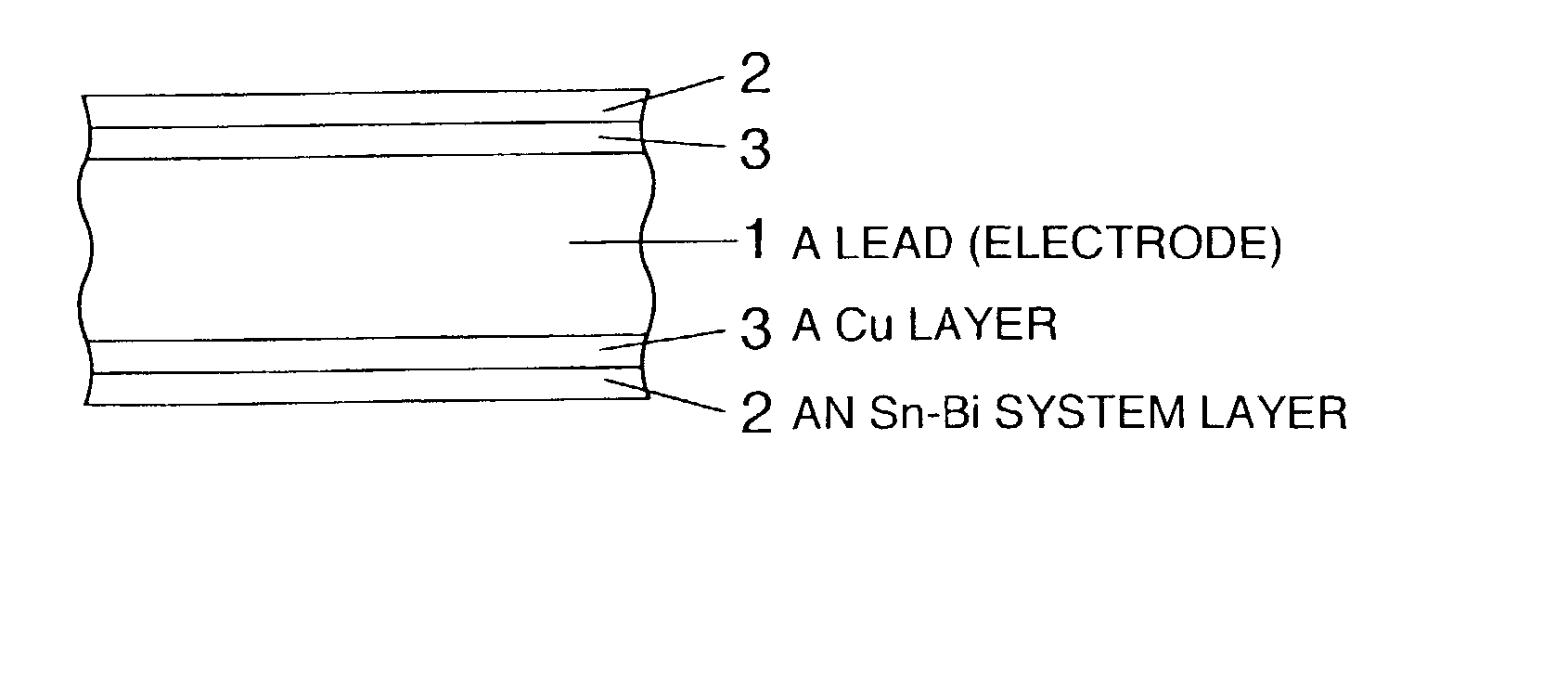
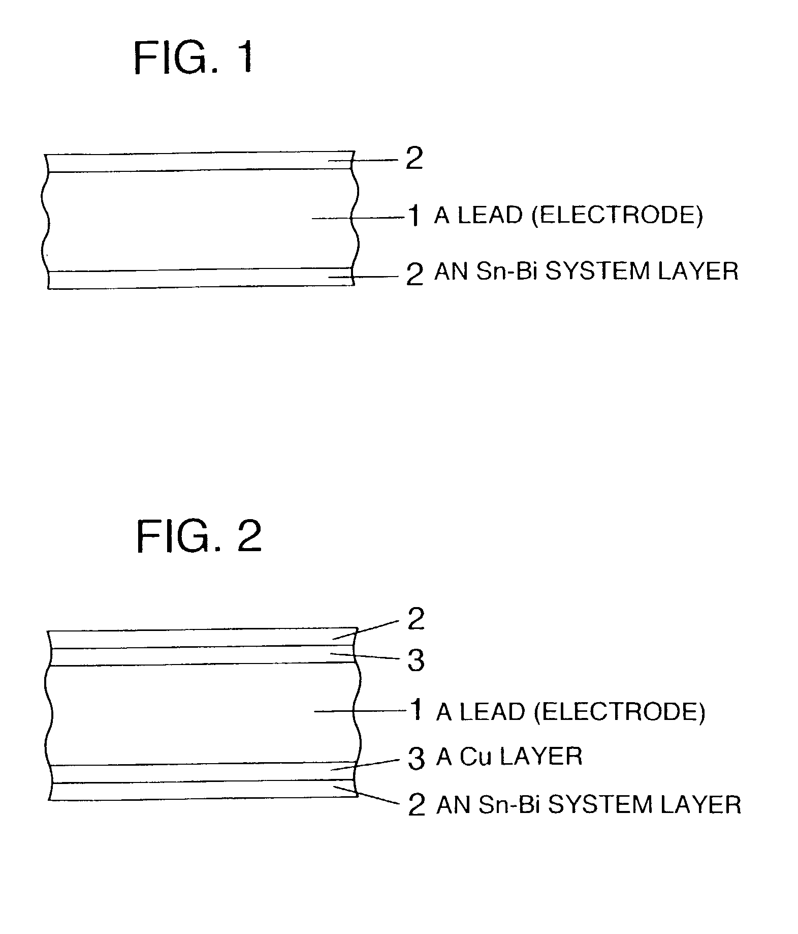
[0053] The cross-sectional structure of a TSOP lead is shown in FIG. 2 which is a part of the lead structure. A Cu layer 3 is formed on a lead 1 which is of an Fe--Ni alloy (42 alloy) and an Sn--Bi alloy layer 2 is formed on this Cu layer. The Sn--Bi alloy layer 3 and Sn--Bi layer 2 were formed by plating. The thickness of the Cu layer 3 was about 8 .mu.m and that of the Sn--Bi plating layer was about 10 .mu.m. The Bi content of Sn--Bi alloy plating layer was 5 wt %. Because of high rigidity of the TSOP lead, when it is used at a high temperature or under a condition that heat generation occurs in the device itself, stress generated at the interface is greater as compared with the QFP-LSI. In such cases, it is necessary to form an interface with sufficient bonding strength high enough to withstand this interface stress and the Cu layer under the Sn--Bi layer is effective for this purpose.

[0054] The TSOP was soldered to a printed-circuit board in a vapor reflow furnace with utilizati...

example 3

[0055] The electrode structures according to this invention can also be applied in an electrode on a board. For example, solder coating is effective in improving the solderability of boards. Conventionally, there have been used lead-containing solders such as a eutectic Sn--Pb alloy solder. Thus, the Sn--Bi alloy layer according to the invention can be used to make the solder for coating lead-free. Furthermore, because the electrode of a board is made of copper, sufficient bonding strength can be obtained when an Sn--Ag--Bi alloy solder is used. An example in which this structure is applied is shown; an Sn-8Bi alloy layer of about 5 .mu.m was formed by roller coating on a Cu pad (Cu electrode) on a glass epoxy substrate, which is a circuit board,

[0056] Wettability to boards and bonding strength were improved, because the solder layer was formed.

Industrial Applicability

[0057] An electrode structure can be realized, which is suitable for an Sn--Ag--Bi alloy solder excellent as a lead-...


PUM

PropertyMeasurementUnit
thicknessaaaaaaaaaa
melting pointaaaaaaaaaa

Abstract

Provided are a bonded structure by a lead-free solder and an electronic article comprising the bonded structure. The bonded structure has a stable bonding interface with respect to a change in process of time, an enough strength and resistance to occurrence of whiskers while keeping good wettability of the solder. In the bonded structure, a lead-free Sn-Ag-Bi alloy solder is applied to an electrode through an Sn-Bi alloy layer. The Sn-Bi alloy, preferably, comprises 1 to 20 wt % Bi in order to obtain good wettability of the solder. In order to obtain desirable bonding characteristics having higher reliability in the invention, a copper layer is provided under the Sn-Bi alloy layer thereby obtaining an enough bonding strength.

Description

[0001] The present invention relates to a bonded structure by a lead-free solder, in which an electronic device is bonded to an electrode of a lead frame, etc. by means of the lead-free solder of low toxicity, and an electronic article with the bonded structure.[0002] In order to produce an electric circuit board by bonding electric devices (e.g. LSIs) to a circuit board made of an organic material, for example, conventionally, there has been used a eutectic Sn--Pb alloy solder, another Sn--Pb alloy solder which has a chemical composition and a melting point each close to that of the eutectic Sn--Pb alloy solder, and other solder alloys which are obtained by adding small amounts of bithmuth (Bi) and / or silver (Ag) to the solders recited above. These solders comprise about 40 wt % Pb and have a melting point of about 183.degree. C., which permit soldering at 220-240.degree. C.[0003] With regard to electrodes of electronic devices, such as QFP (Quad Flat Package)-LSIs, to be soldered,...

Claims


Application Information

Patent Timeline
Patent Type & Authority Applications(United States)
IPC IPC(8): B23K1/00B23K35/00B23K35/26C22C13/02H01L23/50H05K3/34
CPCB23K1/0016Y10T428/12708B23K35/007B23K35/262B23K2201/40H01L23/488H01L23/49811H01L23/532H05K3/3426H05K3/3463H05K2201/10909H05K1/181H01L2924/01322H01L24/29H01L2224/83101Y10T29/49144Y10T29/49149Y10T29/49169Y10T428/12715B23K35/004B23K2101/40H01L2924/15747Y02P70/50H01L2924/00
Inventor SHIMOKAWA, HANAESOGA, TASAOOKUDAIRA, HIROAKIISHIDA, TOSHIHARUNAKATSUKA, TETSUYAINABA, YOSHIHARUNISHIMURA, ASAO
Owner RENESAS ELECTRONICS CORP
Why Eureka
Try Eureka