Metal coordination compound, luminescence device and display apparatus

a technology of luminescence device and coordination compound, which is applied in the direction of discharge tube luminescnet screen, other domestic articles, natural mineral layered products, etc., can solve the problems of material change or life deterioration, high probability of deactivation process, and limited luminescence efficiency to at most 25%
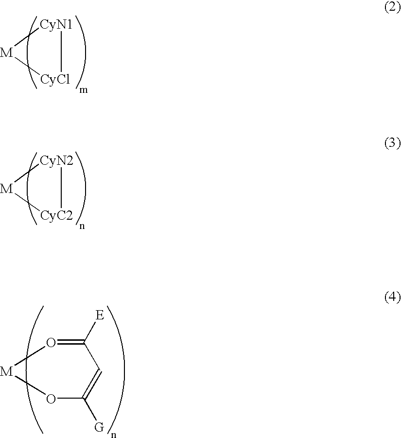
Inactive Publication Date: 2003-05-08
CANON KK
View PDF0 Cites 41 Cited by
  • Summary
  • Abstract
  • Description
  • Claims
  • Application Information

AI Technical Summary

Problems solved by technology

Conventional organic EL devices have utilized fluorescence of which the luminescence efficiency is limited to at most 25%.
More specifically, because it is held in a high-energy excited state for a longer period, it is liable to react with surrounding materials and cause polymer formation among the excitons, thus incurring a higher probability of deactivation process resulting in a material change or life deterioration.
More specifically if the phosphorescence life is long, the number of triplet state molecules maintained for luminescence is increased, and the deactivation process is liable to occur, thus resulting in a lower luminescence efficiency particularly at the time of a high-current density.
%, a resultant luminescence strength is undesirably be lowered due to quenching with an increasing concentration in some cases.

Method used


Image

  • Metal coordination compound, luminescence device and display apparatus
  • Metal coordination compound, luminescence device and display apparatus
  • Metal coordination compound, luminescence device and display apparatus

Examples


examples 2-10

[0117] Each of luminescence devices having a layer structure shown in FIG. 1B were prepared in the following manner.

[0118] On a 1.1 mm-thick glass substrate (transparent substrate 15), a 100 nm-thick film (transparent electrode 14) of ITO (indium tin oxide) was formed by sputtering, followed by patterning to form a stripe electrode including 100 lines each having a width of 100 nm and a spacing with an adjacent line of 10 nm (i.e., electrode pitch of 110 nm).

[0119] On the ITO-formed substrate, three organic layers and two metal electrode layers shown below were successively formed by vacuum (vapor) deposition using resistance heating in a vacuum chamber (10.sup.-4 Pa).

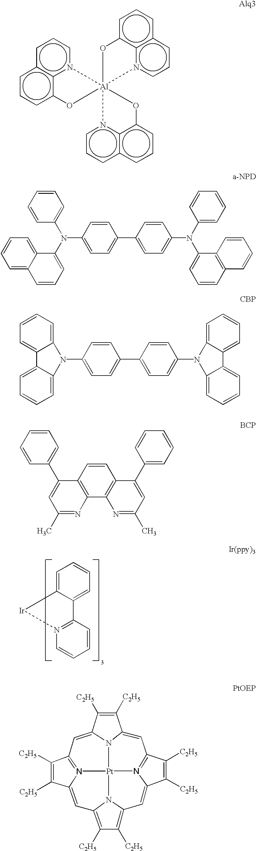
[0120] Organic layer 1 (hole transport layer 13) (40 nm): .alpha.-NPD

[0121] Organic layer 2 (luminescence layer 12) (30 nm): co-deposited film of CBP:metal complex (metal coordination compound shown in Table 18) (95:5 by weight)

[0122] Organic layer 3 (electron transport layer 16) (30 nm): Alq3

[0123] Metal electrode lay...

example 11

[0132] A color organic EL display apparatus shown in FIG. 2 was prepared in the following manner.

[0133] An active matrix substrate had a planar structure basically similar to a structure described in U.S. Pat. No. 6,114,715.

[0134] Specifically, on a 1.1 mm-thick glass substrate, top gate-type TFTs of polycrystalline silicon were formed in an ordinary manner and thereon, a flattening film was formed with contact holes for electrical connection with a pixel electrode (anode) at respective source regions, thus preparing an active matrix substrate with a TFT circuit.

[0135] On the active matrix substrate, a 700 nm-thick pixel electrode (anode) of ITO having a large work function was formed in a prescribed pattern. On the ITO electrode, prescribed organic layers and a 100 nm-thick Al electrode (cathode) were successively formed by vacuum deposition with a hard mask, followed by patterning to form a matrix of color pixels (128.times.128 pixels).

[0136] The respective organic layers correspo...

example 12

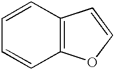
Synthesis of Ex. Comp. No. 31

[0141] It is easy to synthesize the following compound in the same manner as in Example 1 except for using 2-bromopyridine (made by Tokyo Kasei Kogyo K.K.) instead of 2-chloro-5-trifluoromethylpyridine in Example 1.

[0142] Tris[2-(benzofuran-2-yl)pyridine-C.sup.3,N]iridium (III).


PUM

PropertyMeasurementUnit
excitation wavelengthaaaaaaaaaa
widthaaaaaaaaaa

Abstract

An electroluminescence device having a layer containing a specific metal coordination compound is provided. The metal coordination compound is represented by formula (1) below:MLmL'n (1),wherein M is a metal atom of Ir, Pt, Rh or Pd; L and L' are mutually different bidentate ligands; m is 1, 2 or 3 and n is 0, 1 or 2 with the proviso that m+n is 2 or 3; a partial structure MLm is represented by formula (2) shown below and a partial structure ML'n is represented by formula (3) or (4) shown below: at least one of the optional substituent(s) of the cyclic groups, and the cyclic groups CyC1 and CyC2 includes a benzofuran structure capable of having a substituent represented by the following formula (5): The metal coordination compound having the benzofuran structure is effective in providing high-efficiency luminescence and long-term high luminance.

Description

FIELD OF THE INVENTION AND RELATED ART[0001] The present invention relates to an organic luminescence device (also called an organic electroluminescence device or organic EL device) for use in a planar light source, a planar display, etc. Particularly, the present invention relates to a novel metal coordination compound and a luminescence device having a high luminescence efficiency and causing little change with time by using a metal coordination compound represented by formula (1) appearing hereinafter.[0002] An old example of organic luminescence device is, e.g., one using luminescence of a vacuum-deposited anthracene film (Thin Solid Films, 94 (1982) 171). In recent years, however, in view of advantages, such as easiness of providing a large-area device compared with an inorganic luminescence device, and possibility of realizing desired luminescence colors by development of various new materials and drivability at low voltages, an extensive study thereon for device formation as ...

Claims


Application Information

Patent Timeline
Patent Type & Authority Applications(United States)
IPC IPC(8): C07F15/00C09K11/06H01L51/00H01L51/50H01L51/30
CPCC07F15/0033C09K11/06C09K2211/1007C09K2211/1011C09K2211/1014C09K2211/1029Y10S428/917C09K2211/185H01L51/0084H01L51/0085H01L51/0087H01L51/5012C09K2211/1088H10K85/341H10K85/346H10K85/342H10K50/11
Inventor TAKIGUCHI, TAKAOOKADA, SHINJIROTSUBOYAMA, AKIRAMIURA, SEISHIMORIYAMA, TAKASHIKAMATANI, JUNFURUGORI, MANABU
Owner CANON KK
Why Eureka
Try Eureka