

Resist pattern thickening material, resist pattern and forming method thereof, and semiconductor device and manufacturing method thereof
a technology of resist pattern and thickening material, which is applied in the direction of photomechanical equipment, photosensitive material processing, instruments, etc., can solve the problems of inability to efficiently perform resist pattern thickening, inferior etching resistance of arf resist thickened by film, and inability to suitably use material, method or the lik
- Summary
- Abstract
- Description
- Claims
- Application Information
AI Technical Summary
Benefits of technology
Problems solved by technology
Method used
Image

Examples
example 1
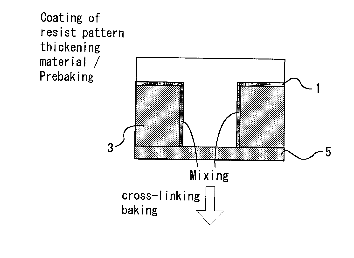
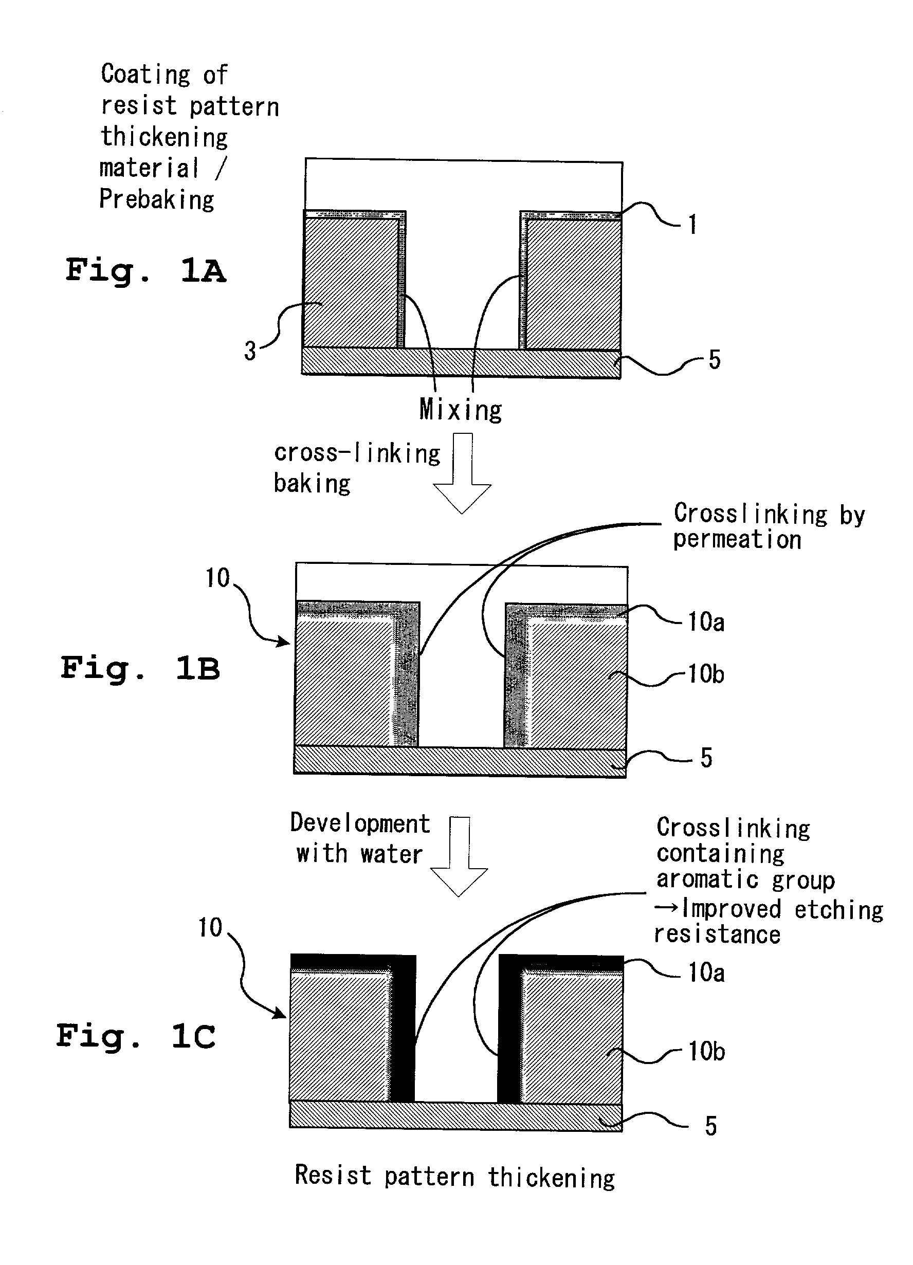
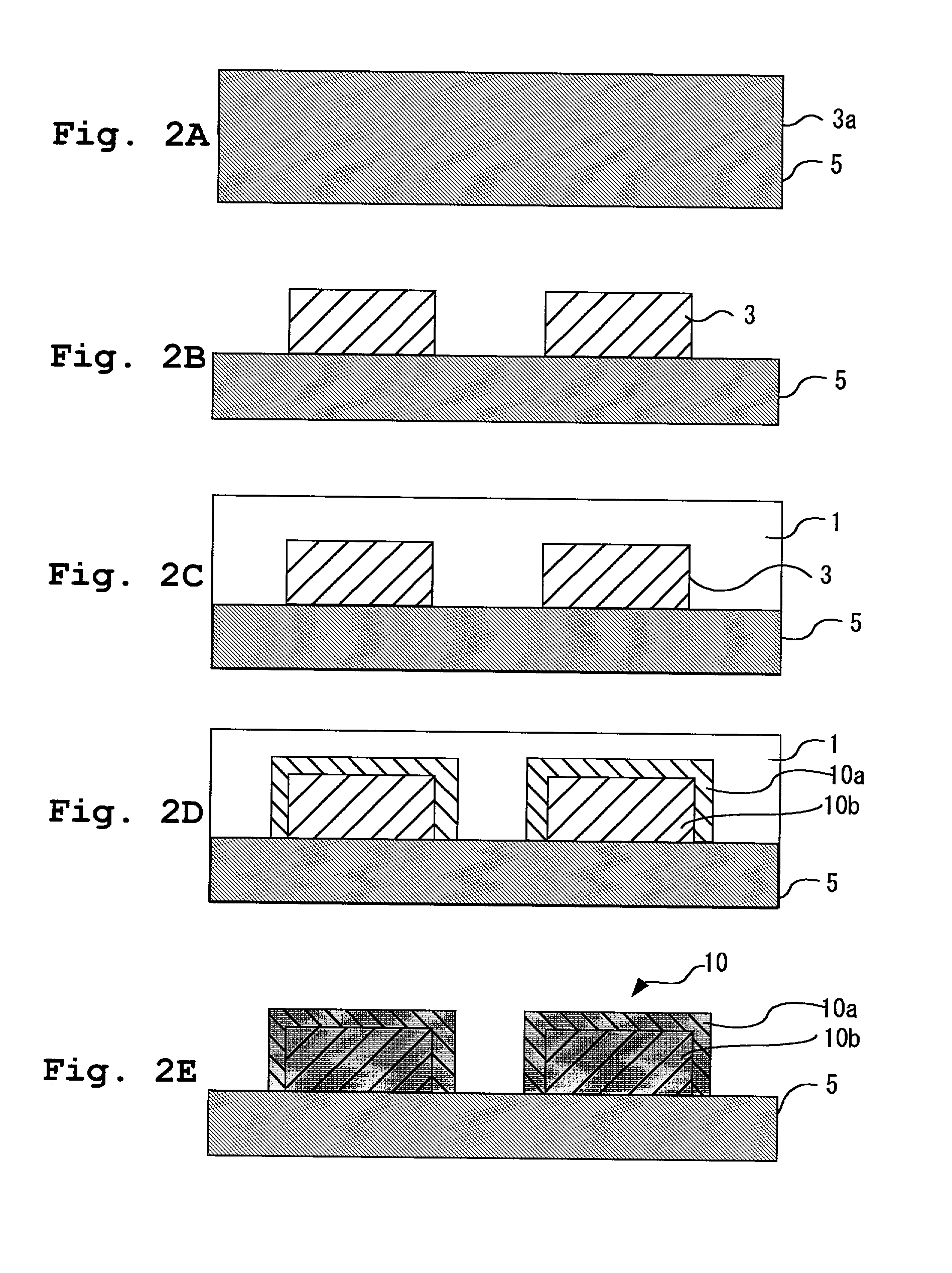
[0151] Preparation of Resist Pattern Thickening Material
[0152] Resist pattern thickening materials A-I according to the present invention having compositions shown in Table 1 were prepared. In Table 1, the unit of the numeric in parentheses represents a part by mass. In the column of "Resin", "KW3" represents a polyvinyl acetal resin (manufactured by SEKISUI CHEMICAL), and "PVA" shows a polyvinyl alcohol resin (manufactured by KURARAY, Poval 117). In the column of "Crosslinking agent", "Uril" represents tetramethoxymethyl glycouril, "Urea" represents N, N'-dimethoxymethyl dimethoxyethyleneurea, and "Melamine" represents hexamethoxymethylmelamine. In the column of "Surfactant", "TN-80" represents a nonionic surfactant (manufactured by ASAHI DENKA, polyoxyethylene monoalkyl ether surfactant). As the main solvent component except the above resin, crosslinking agent, and water-soluble aromatic compound, a mixture of pure water (deionized water) and isopropyl alcohol (mass ratio of pure ...
example 2
[0163] Flash Memory and Its Manufacture
[0164] Example 2 is one embodiment of the semiconductor device and manufacturing method thereof of the present invention using the resist pattern thickening material of the present invention. In Example 2, resist films 26, 27, 29, 32 and 34 are thickened by use of the resist pattern thickening material of the present invention according to the same method as in Example 1.
[0165] FIGS. 3A and B are upper surface views (plan views) of a FLASH EPROM called FLOTOX type or ETOX type. FIGS. 4A to 4C, FIGS. 5D to 5F, and FIGS. 6G to 61 are schematic sectional views for showing one example for the manufacturing method for the FLASH EPROM, wherein the left views in FIGS. 4A through 61 are schematic sectional (A-directional sectional) views in the gate lateral direction (X-direction in FIG. 3A) of the part for forming a MOS transistor having a floating gate electrode in a memory cell pat (first element region), the central views are schematic sectional (B...
example 3
[0189] Manufacture of Magnetic Head
[0190] Example 3 relates the manufacture of a magnetic head as an applied example of the resist pattern according to the present invention using the resist pattern thickening material according to the present invention. In Example 3, resist patterns 102 and 126 are thickened by the same method as in Example 1 by use of the resist pattern thickening material according to the present invention.
[0191] FIGS. 9A through D are flowcharts for showing the manufacture of the magnetic head.
[0192] A resist film was formed on an underlayer insulation layer 100 in a thickness of 6 .mu.m, as shown in FIG. 9A, followed by exposure and development to form a resist pattern 102 having an opening pattern for forming a spiral thin film magnetic coil.
[0193] A plating underlying layer 106 comprising the lamination of a Ti adhesion layer 0.01 .mu.m thick and a Cu adhesion layer 0.05 .mu.m thick was formed by evaporation, as shown in FIG. 9B, on the resist pattern 102 and...
PUM
| Property | Measurement | Unit |
|---|---|---|
| wavelength | aaaaa | aaaaa |
| wavelength | aaaaa | aaaaa |
| boiling point | aaaaa | aaaaa |
Abstract
Description
Claims
Application Information