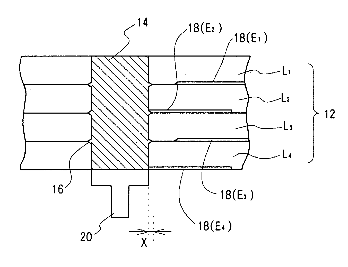
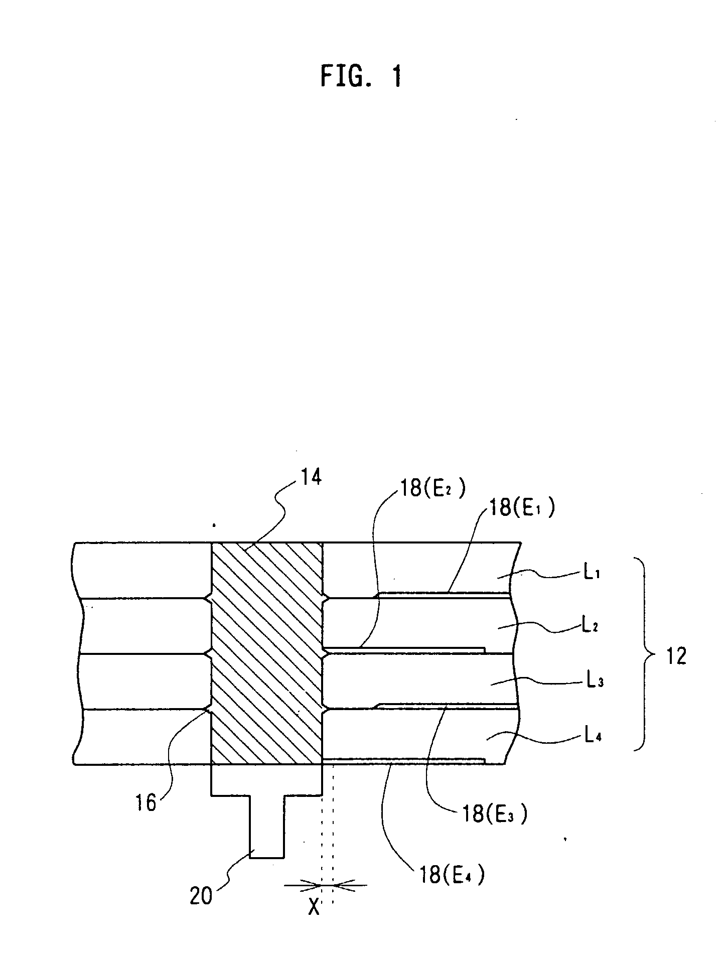
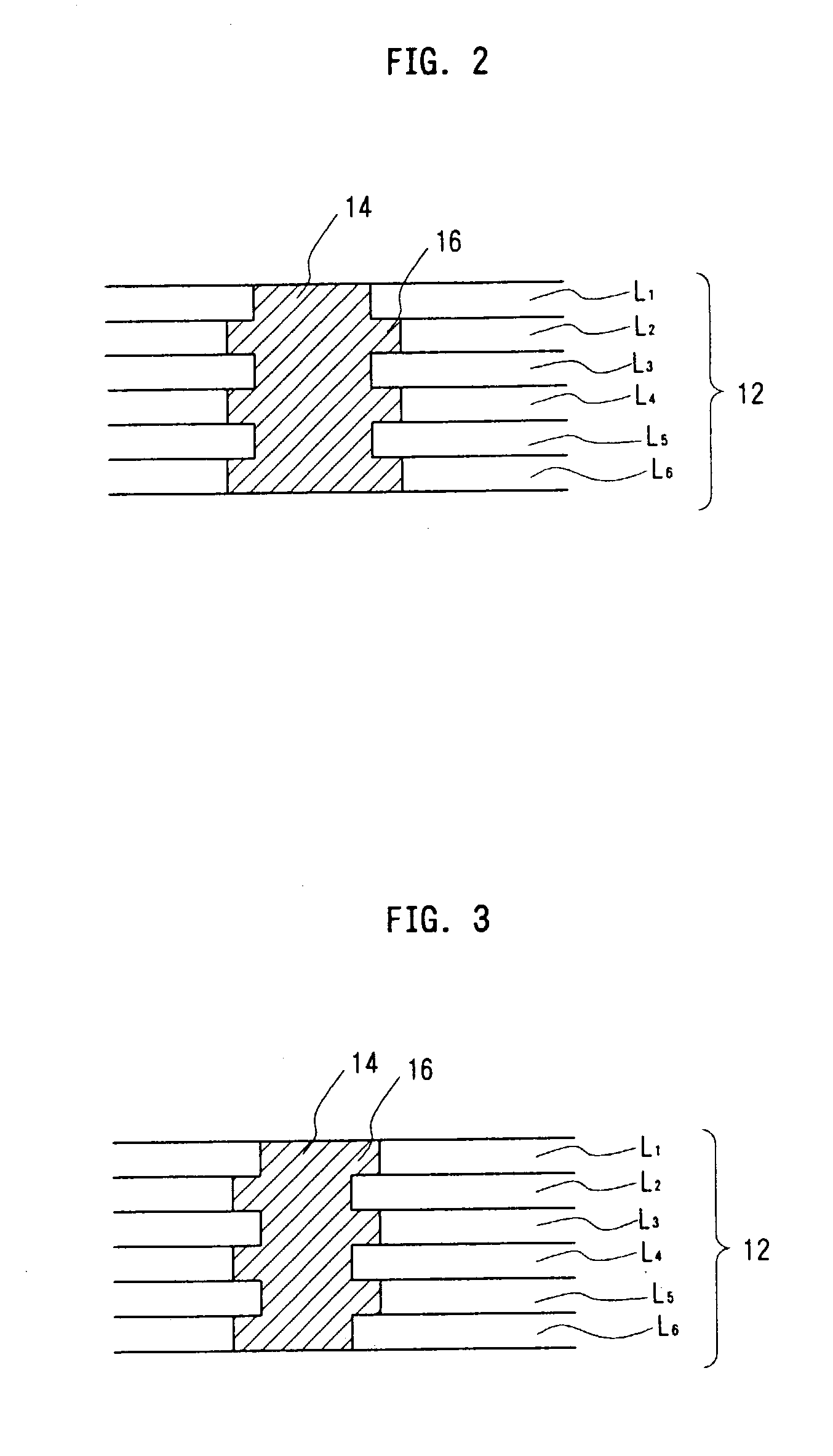
Ceramic substrate

a ceramic substrate and substrate technology, applied in the field of ceramic substrates, can solve the problems of deterioration of adhesion between through-holes tungsten and sintered ceramic materials tending to deteriorate, and high cost, and achieve excellent reliability performance, high reliability performance, and excellent tolerance against drawing stress

Inactive Publication Date: 2003-06-05
IBIDEN CO LTD
View PDF19 Cites 23 Cited by
  • Summary
  • Abstract
  • Description
  • Claims
  • Application Information

AI Technical Summary

Benefits of technology

0090] The ceramic substrate according to claims 1 to 4 consistent with the present invention allows the through-hole structure to have excellent tolerance against a drawing stress applied to an external terminal pin, and to have excellent reliability performance. Furthermore, it is difficult to cause a hot spot to be formed, thereby achieving uniform distribution of temperatures. According to the present invention, an electrostatic chuck, a wafer prober and a heater that have above-mentioned through hole structure can be manufactured easily. These products achieve high reliability performance against a drawing stress applied to an external terminal pin and further achieve uniform distribution of the temperatures.

Problems solved by technology

Accordingly, adhesion between tungsten and sintered ceramic materials tends to deteriorated.
Due to a long-term use, if a heat sink cycle and a thermal shock are applied to such electrostatic chuck, adhesion between the through-hole and a sintered ceramic material deteriorates.
The structure arises a problem such that the repeated attachment and detachment between the external terminal pin and a power supply causes a drawing force to be applied to the through-hole, thus resulting that adhesion between a through-hole and a sintered ceramic material to be deteriorated.

Method used


Image

  • Ceramic substrate
  • Ceramic substrate
  • Ceramic substrate

Examples


example 2

(EXAMPLE 2)

An Electrostatic Chuck with a Heater

[0074] (1) A paste was made by mixing 100 parts by weight of powdered aluminium nitride, 4 parts by weight of yttrium (a mean particle diameter 0.4 .mu.m), 11.5 parts by weight of acrylic binder, 0.5 part by weight of dispersant, and 53 parts by weight of alcohol mixture containing 1-butanol and ethanol. By means of the doctor blade method, the sheet formation was made from the paste to obtain a green sheet having a thickness of 0.47 mm.

[0075] (2) Thus prepared green sheet was dried at 80.degree. C. for five hours. After that the passing through-holes 44 having a diameter of 3.0 mm, being used for inserting a pin for supporting a semiconductor wafer were formed by way of punching; and the through-holes 14 for connection with the external pin having a diameter of 5.0 mm were formed by way of punching.

[0076] (3) Conductive paste A was prepared by mixing 100 parts by weight of tungsten carbide having a mean particle diameter of 1 .mu.m, 3....


PUM

PropertyMeasurementUnit
temperatureaaaaaaaaaa
diameteraaaaaaaaaa

Abstract

The present invention provides a ceramic substrate for use in an apparatus for manufacturing and inspecting semiconductors. The ceramic substrate comprises a through-hole having excellent tolerance performance against a drawing stress applied to an external terminal pin. The through-hole is provided with a projection which protrudes into the ceramic substrate made of aluminum nitride as primary component.

Description

[0001] The present invention relates to a ceramic substrate for use in the semiconductor industrial field, and more particularly, it relates to a ceramic substrate for use in a wafer prober, an electrostatic chuck, a hot plate and the like, for use in the manufacture or inspection processes of semiconductors.[0002] Applied semiconductor products are indispensable in many industrial fields. As a typical example, semiconductor chips are manufactured by slicing a silicon monocrystalline to a predetermined thickness to produce a silicon wafer; then forming a variety of circuits in a pattern shape thereon.[0003] In order to manufacture a semiconductor chip, an electrostatic chuck for supporting a wafer, a hot plate for heating a wafer, and a wafer prober for checking whether the circuit operates in accordance with its design are needed. These may preferably be of ceramic material in terms of heat resistance and corrosion resistance.[0004] For example, Japanese patent registration No. 279...

Claims


Application Information

Patent Timeline
Patent Type & Authority Applications(United States)
IPC IPC(8): H01L21/683H01L23/498H02N13/00
CPCH01L21/6833H01L23/49827H02N13/00Y10T428/24926H01L2924/0002Y10T428/24917H01L2924/00
Inventor ITO, YASUTAKA
Owner IBIDEN CO LTD
Why Eureka
Try Eureka