1. General-purpose microcomputers (GPMCs). GPMCs (such as the
Pentium line from Intel, and the
PowerPC series from Motorola and IBM) have been adapted to maximize
throughput at the expense of latency. Latency is the
delay through the GPMC
chip between input and output data for a single operation. Latency is long because the data is grouped with other data going into and out of the
chip, and the operation is embedded in a pipeline with many stages of other operations. Almost all computers have a
memory hierarchy; for example, a small amount of fast SRAM registers at the top of the hierarchy,
a moderate amount of slower
system memory in the middle of the hierarchy, and a large amount of very slow disk-drive-based storage at the bottom. In GPMCs each processor may have a
register file for data, an instruction issue unit, and a level-one (L1) cache. The L1 cache may be split between instructions and data or may be unified. Caches improve performance because of the locality of references in most computer programs, i.e., the tendency of the next operation to reference a memory location nearby the last-referenced memory location. A level-2 (L2) cache is usually needed to interface with main memory (larger, slower, cheaper dynamic RAM chips). Many GPMC chips support single-instruction-multiple-data (
SIMD) parallelism through several execution units; some of the largest chips support multiple instruction streams for
MIMD behavior. In a GPMC with multiple execution units, the L2 cache is usually shared among execution units, with some "cache-coherence" scheme to prevent loss of data when writing to this
shared memory. An L3 cache may be used if the main memory is relatively much slower. Additional controllers for memory and I / O channels may be integrated on the same
chip. The general-purpose programmability and large market for GPMCs allows them to be
mass-produced and sold at low
unit cost. The disadvantages of the GPMC and its complex of caches and pipelines include relatively high power dissipation and the aforementioned relatively large latencies from when data enters the CPU to when results are output.
2.
Digital signal processors (DSPs). DSPs may be divided into classes according to whether the ALU uses fixed-point or floating-point numbers, and also by the number of ALUs per IC chip. Power dissipation per operation is usually less for DSPs than GPMCs due to the use of specialized instructions to facilitate
signal processing. DSPs may exhibit less latency than GPMCs for a given operation due to fewer cache
layers and shorter pipelines. Instruction words may be longer, permitting explicit parallel execution, compared to automatic / speculative parallel execution in the GPMCs. Higher performance DSP implementations may support parallelism through multiple execution units, and in general, DSPs require fewer support chips than GPMCs. The large market for DSPs allows them to be
mass-produced at low cost. In the DSP market there is demand for ICs that perform fixed-point arithmetic only, as well as for ICs that support both fixed- and floating-point operations. The disadvantages of DSPs include greater difficulty of
programming, and poorer performance on certain types of algorithms.
3. Field-programmable gate arrays (FPGAs). FPGAs are digital ICs, which can be programmed or customized by users "in the field" as opposed to during
wafer fabrication. FPGAs may be classified by the number of logic gates they contain, and in the more recent, largest versions, by the number of ALUs and memory on the IC. Theoretically all the FPGA ALUs can compute in parallel, following a
SIMD or
MIMD or mixed control paradigm. Customizing an FPGA is similar to
programming a DSP / GPMC, but arriving at the desired program is more difficult, generally requiring engineers who are knowledgeable in logic design, and specialized design
automation tools. However, if speed is more important than power dissipation, FPGAs often provide faster
processing than DSP / GPMCs. Although
mass-produced, large FPGAs are several times more expensive than GPMC chips with the same number of gates.
4.
Application specific integrated circuits (ASICs). ASICs are customized to specific applications by designing specific circuit layouts which may range from
full custom circuits to hierarchical integration of
library modules.
Library modules may range from individual logic gates and I / O cells to memory arrays and
microprocessor cores. Performance can be higher than GPMC / DSP / FPGA approaches because the ASIC hardware is tailored to the algorithms required by the application. Speed can also be faster than a FPGA because the configuration circuits can be eliminated, resulting in a more compact
layout with lower parasitic capacitances. The development costs for an ASIC are much higher than any other approach, running from several to tens of millions of dollars (and higher for complex video chips). Millions of chips of a particular design may need to be sold to amortize the high costs of developing one.
All of these components have latency due to internal delays, and these latencies grow with the size of the component and number of input / output ports on it.
There are several problems with this parallel architecture when two or more processors are working the same task.
Both bandwidth and latency of the L2 cache are adversely affected by increased capacity.
However, the number of wires in fully-connected network increases as N.sup.2 / 2 where N is the number of ports, and thus a fully-connected network quickly becomes impractical for even medium sized systems.
However, certain applications require a much greater level of performance or computational
throughput than is possible using current systems.
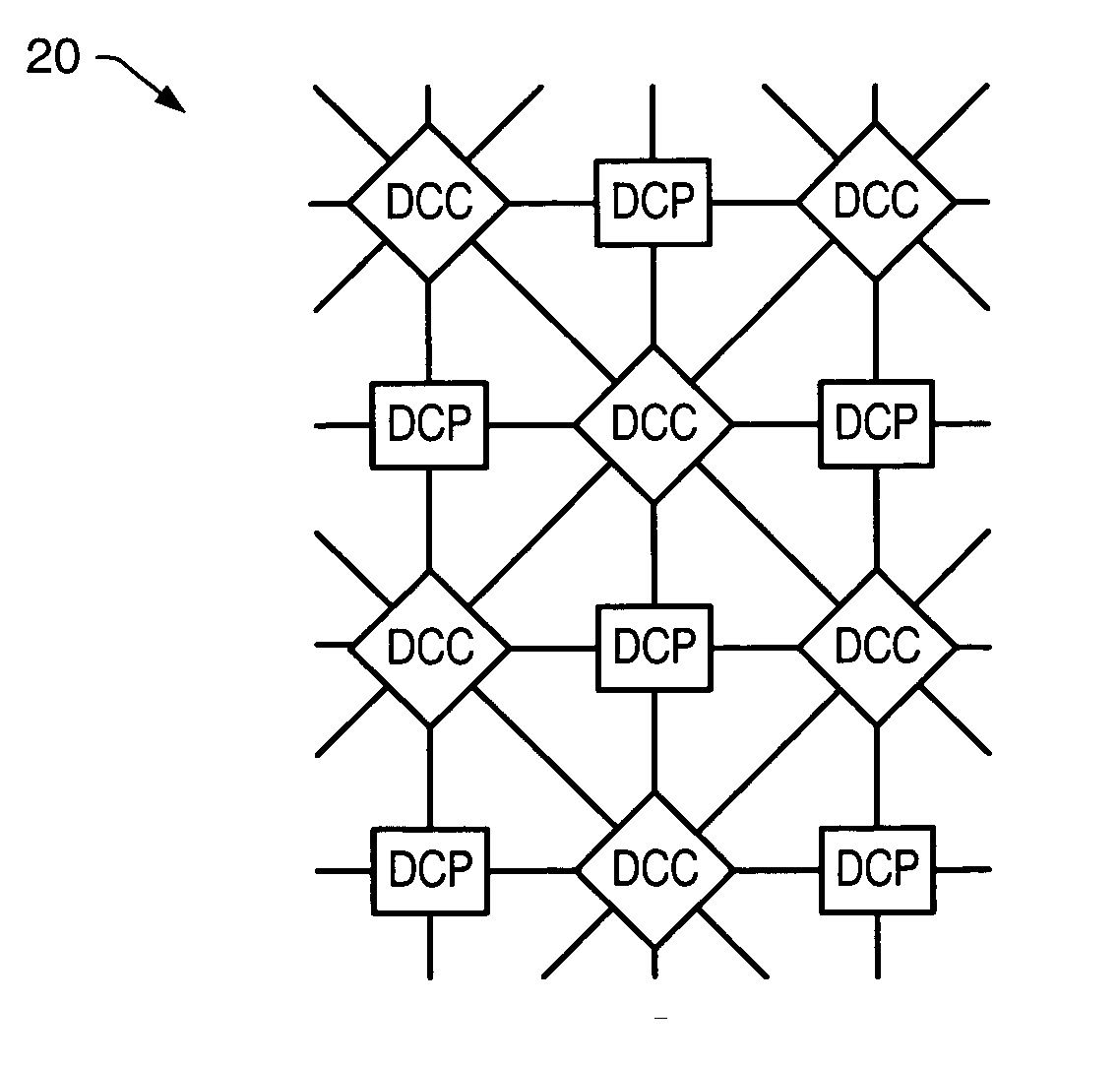
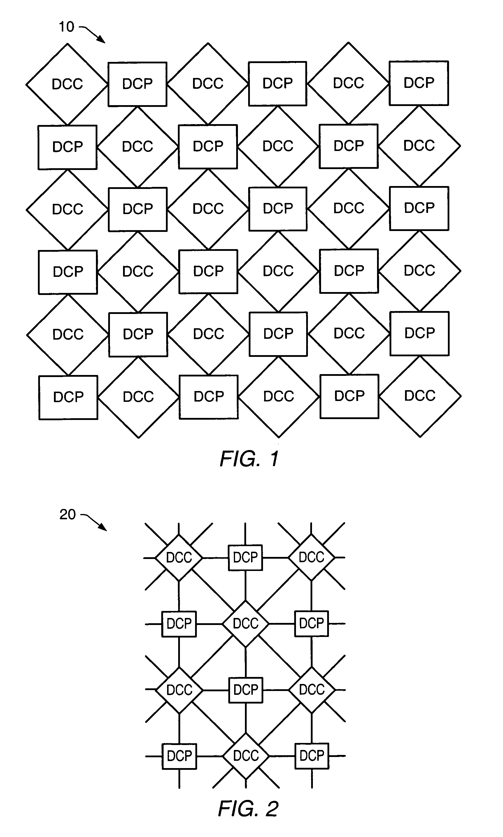
Such a pair may be logically adjacent but not physically adjacent, and the
signal propagation time from the one DCC to the other may be too great to satisfy the latency requirement of neighbors.
Access from the one DCC to the other DCC may
traverse one or more intermediate nodes, and the resulting transit
delay may be too great to satisfy the latency requirement of neighbors.
In a dynamic environment where pathways are frequently created and destroyed, a large number of crossbar configuration codes may be required, storage of which may in turn consume potentially limited DCC RAM resources.
Increased IC packaging may require additional space, and interconnections through and around IC packaging may incur delays that are proportional to
path length.
However, for longer distances and larger amounts of data, many moves may be required to transport data and many DCPs may therefore spend a majority of cycles simply moving data instead of performing more useful arithmetic.
When mapping a flow diagram to the
MMAP, communication delays between DCP / DCC nodes that are proportional to the distances between nodes may arise.
For many SRAM implementations, a memory access error may also occur if the same location is simultaneously read to and written from.
However,
software and hardware design may take such desynchronization potential into account, providing sufficient instruction bandwidth such that potentially desynchronized program threads may perform
handshaking steps with other processes.
In various embodiments the hardware may or may not prevent pathways from being interrupted once established.
However, the production and consumption of data by the source and destination DCCs may be uneven.
In such a case, if the destination node is not advised that data arrival has stopped, it may incorrectly continue processing.
However, if the source node stalls and the destination node continues processing the buffer contents, the destination node may incorrectly process stale data as though it were new data.

