Method of producing electronic device material

a technology for electronic devices and materials, applied in the direction of coatings, chemical vapor deposition coatings, electric discharge tubes, etc., can solve the problems of deterioration of the quality of the resultant electronic device per se, deterioration of the electric characteristics of the layer, and relatively noticeable defects in the film, etc., to achieve low electron temperature, high density, and light plasma damage

Inactive Publication Date: 2004-03-11
TOKYO ELECTRON LTD
View PDF4 Cites 270 Cited by
  • Summary
  • Abstract
  • Description
  • Claims
  • Application Information

AI Technical Summary

Benefits of technology

0156] Thus, the plasma which has been formed by irradiating a process gas with microwave by use of an SPA is one having a high density and a relatively low electron temperature. Therefore, the present invention can generate high-density radicals, and the bias between the plasma and the surface of the substrate to be processed can be suppressed to a relatively low value, and the plasma damage is light. Therefore, it is considered that the dangling bonds present in the SiO.sub.2 film can appropriately be terminated by the oxygen reactive species which have been generated by the plasma, and the weak Si--Si bond is changed into a strong Si--O--Si bond, to thereby form an SiO.sub.2 film having a good electric characteristic as shown in FIG. 9 by modification.

Problems solved by technology

However, in the layers formed by the CVD process, the resultant surface roughness, and defects in the film are relatively noticeable, and the valences of atomic bonding called "dangling bonds" are liable to be formed so that the dangling bonds are directed toward the inside of the film.
As a result, there can occur a problem such that electric characteristics of the layer can be deteriorated, and the quality of the resultant electronic device per se can be deteriorated accordingly.

Method used


Image

  • Method of producing electronic device material
  • Method of producing electronic device material
  • Method of producing electronic device material

Examples


second embodiment

[0164] (Second Embodiment)

[0165] Hereinbelow, a second embodiment of the present invention will be described. In this second embodiment, an insulating film is surface-modified with an SPA plasma processing during the process for producing a logic device.

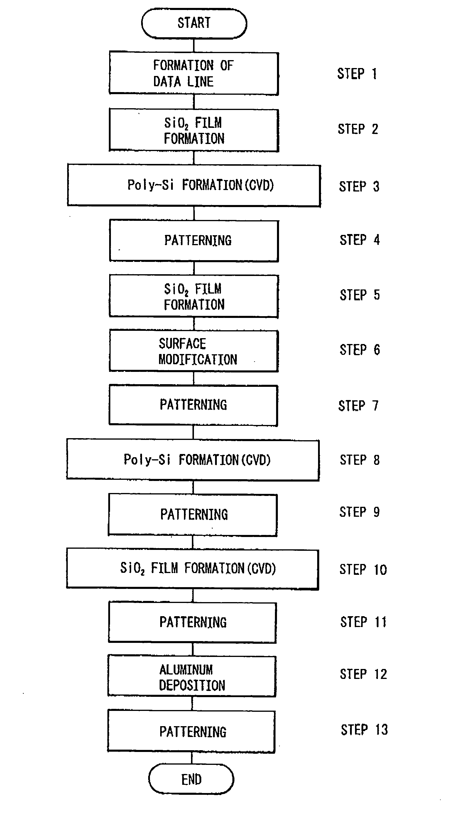
[0166] FIG. 10 is a flowchart showing the manufacturing steps for the logic device relating to this embodiment. FIGS. 11A to 11F are schematic vertical sectional views showing the manufacturing steps for the logic device relating to this embodiment.

[0167] The production steps for the logic device relating to this embodiment can roughly classified into the following flows.

[0168] Element separation (or isolation).fwdarw.MOS transistor fabrication.fwdarw.capacity fabrication.fwdarw.interlayer insulating film formation and wiring (or interconnection).

[0169] Hereinbelow, a general example will be described with respect to the fabrication of an MOS structure which is a preceding process during the fabrication of the MOS transistor includin...


PUM

PropertyMeasurementUnit
temperatureaaaaaaaaaa
pressureaaaaaaaaaa
temperatureaaaaaaaaaa

Abstract

A process for producing an electronic device material of a high quality MOS-type semiconductor comprising an insulating layer and a semiconductor layer excellent in the electrical characteristic. The process includes: a step of CVD-treating a substrate to be processed comprising single-crystal silicon as a main component, to thereby form an insulating layer; and a step of exposing the substrate to be processed to a plasma which has been generated from a process gas on the basis of microwave irradiation via a plane antenna member having a plurality of slots, to thereby modify the insulating film by using the thus generated plasma.

Description

[0001] The present invention relates to a process which is suitably usable for the production of materials to be used for electronic devices. The process for producing a material for electronic device according to the present invention may be used, for example, for forming an MOS-type semiconductor structure.[0002] Hitherto, various kinds of layer-forming techniques have been used in the cases of the formation of plural layers constituting semiconductors or semiconductor materials. Representative examples of these layer-forming techniques may include, e.g., vacuum evaporation processes, sputtering processes, and CVD (chemical vapor deposition) processes. Among these layer-forming techniques, the CVD process has certain characteristics such that it can provide a high film-forming deposition rate for the layer formation, and it can accomplish the film formation within a relatively short period. Accordingly, the CVD process has been used for many steps in the production of various kind...

Claims


Application Information

Patent Timeline
Patent Type & Authority Applications(United States)
IPC IPC(8): C23C16/40C23C16/56H01L21/28H01L21/31H01L21/316H01L21/768H01L29/51
CPCC23C16/401H01L29/518C23C16/56H01J37/3222H01J37/3244H01L21/02164H01L21/02238H01L21/02252H01L21/02255H01L21/02271H01L21/0234H01L21/28185H01L21/28194H01L21/28202H01L21/28273H01L21/3105H01L21/31604H01L21/31612H01L21/31658H01L21/31662H01L21/76826H01L21/76828H01L29/517C23C16/402H01L29/40114H01L21/76801H01L21/20
Inventor SUGAWARA, TAKUYANAKANISHI, TOSHIOOZAKI, SHIGENORIMATSUYAMA, SEIJIMURAKAWA, SHIGEMITADA, YOSHIHIDE
Owner TOKYO ELECTRON LTD
Why Eureka
Try Eureka