

Polymer solution for nanoimprint lithography to reduce imprint temperature and pressure
a technology of imprint lithography and polymer solution, which is applied in the field of polymer solution for nanoimprint lithography to reduce imprint temperature and pressure, can solve the problems of film shrinkage, serious pattern accuracy problems, and damage to circuit functional materials, and achieves low pressure, reduces both imprinting temperature and pressure, and deforms easily
- Summary
- Abstract
- Description
- Claims
- Application Information
AI Technical Summary
Benefits of technology
Problems solved by technology
Method used
Image

Examples
Embodiment Construction
[0015] Reference is made now in detail to specific embodiments, which illustrates the best mode presently contemplated by the inventors for practicing the invention. Alternative embodiments are also briefly described as applicable.
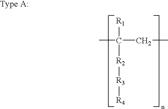
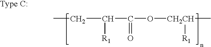
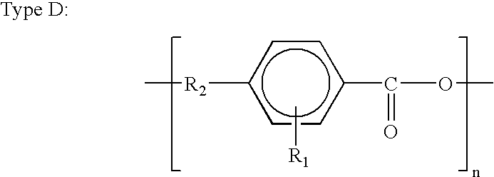
[0016] The present teachings utilize a polymer solution of at least one appropriate polymer dissolved in a polymerizable monomer or monomer mixture. The polymer solution optionally contains one or more initiators, one or more cross-linkers and / or one or more viscosity modifiers. The monomer may be the same or different from the polymer units. If the monomer is the same, then the final polymer film will be relatively pure polymer that is uniform in composition. If the monomer is different from the polymer units, the resulting film may be a polymer blend (i.e., a physical mixture of two different polymers), an interpenetrating network of two polymers, a copolymer (chemical bonding between the two different types of monomer units), or a block co-polymer (regi...
PUM
| Property | Measurement | Unit |
|---|---|---|
| polydispersity | aaaaa | aaaaa |
| polydispersity | aaaaa | aaaaa |
| glass transition temperature | aaaaa | aaaaa |
Abstract
Description
Claims
Application Information