
IC card and booking-account system using the IC card

a technology of ic card and booking account, applied in the field of ic card, can solve the problems of easy forgery, crack or grinding mark, and the misapplication of ic card becomes a bigger problem measurably,

Inactive Publication Date: 2004-07-01
SEMICON ENERGY LAB CO LTD
View PDF88 Cites 105 Cited by
  • Summary
  • Abstract
  • Description
  • Claims
  • Application Information

AI Technical Summary

Benefits of technology

[0014] A third substrate is bonded to the opposite side of the semiconductor element in the first substrate in order to enhance rigidity of the first substrate. When the rigidity of the first substrate is higher than that of the second substrate, the first substrate can be peeled off smoothly with fewer damages to the semiconductor element. However, the third substrate is not always required to be bonded to the first substrate as long as the rigidity of the first substrate is high enough when the first substrate is peeled off from the semiconductor element in a later process.
[0015] The metal oxide film is crystallized by a heat treatment or the like to enhance brittleness thereof and make peeling of the substrate from the semiconductor element easy. The first substrate and the third substrate are together peeled off from the semiconductor element. The heat treatment for crystallizing the metal oxide film may be performed before bonding the third substrate or before bonding the second substrate. Alternatively, a heat treatment performed in a process of forming a semiconductor element may also serve as the process for crystallizing the metal oxide film.
[0024] According to the present invention, an ultrathin film integrated circuit having a total thickness of from 1 .mu.m through 5 .mu.m, typically, 2 .mu.m can be formed by using a thin semiconductor film having a film thickness of 500 nm or less, although an integrated circuit formed using a silicon wafer has a thickness of about 50 .mu.m. The thickness of a display device can be set to about 0.5 mm, preferably, about 0.02 mm. Accordingly, it is possible to provide a display device for an IC card having a thickness of from 0.05 mm through 1 mm. It is also possible to provide a larger number of thin film integrated circuits having a larger circuit scale or a larger memory capacity within the limited area, thereby realizing multi-functionality of the IC card without preventing miniaturization and weight saving of the IC card.
[0025] According to the present invention, a glass substrate that is less expensive and larger than a silicon wafer can be used, and thus, thin film integrated circuits can be mass-produced at low cost and with high throughput. As a result, a manufacturing cost can be reduced dramatically. Further, it is possible to use a substrate repeatedly, thereby reducing the cost.
[0027] A thin film integrated circuit or a display device can be bonded in accordance with a shape of a printed wiring board, and thus, there is a lot of flexibility for a shape of an IC card. Therefore, for example, it is possible to form an IC card into a shape having a curved surface, which can be attached to a columnar bottle.
[0028] The thin film integrated circuit is not limited to a mode in which the thin film integrated circuit is directly equipped for a printed wiring board as a bare chip. The thin film integrated circuit can adopt a mode in which the thin film integrated circuit is mounted on an interposer, packaged and equipped. A smaller and lighter thin film integrated circuit can be obtained by being equipped a thin film integrated circuit as a bare chip. On the other hand, equipment can be performed easily by being equipped after packaging, without requiring a clean room or a special technology or facility such as a bonder when a thin film integrated circuit provided by a packaging manufacturer is equipped on an electronic device manufacturer side. The thin film integrated circuit can be protected from an external environment, standardization of a footprint of a printed wiring board can be realized, wirings of a thin film integrated circuit on a sub micron scale can be enlarged to almost the same millimeter scale as a printed wiring board.

Problems solved by technology

As an IC card is used more widely, a misapplication of an IC card becomes a bigger problem measurably.
A future issue is how securely identification is performed when an IC card is used.
However, in general, a picture of a face is transferred to an IC card by a printing method, and thus there is a pitfall that the picture of a face is easily changed by forgery.
The back-grinding process results in a crack or a grinding mark.

Method used


Image

  • IC card and booking-account system using the IC card
  • IC card and booking-account system using the IC card
  • IC card and booking-account system using the IC card

Examples


embodiment 1

[0136] Embodiment 1

[0137] In this embodiment, electrical connection between an interposer provided for a contact type IC card and a thin film integrated circuit is described.

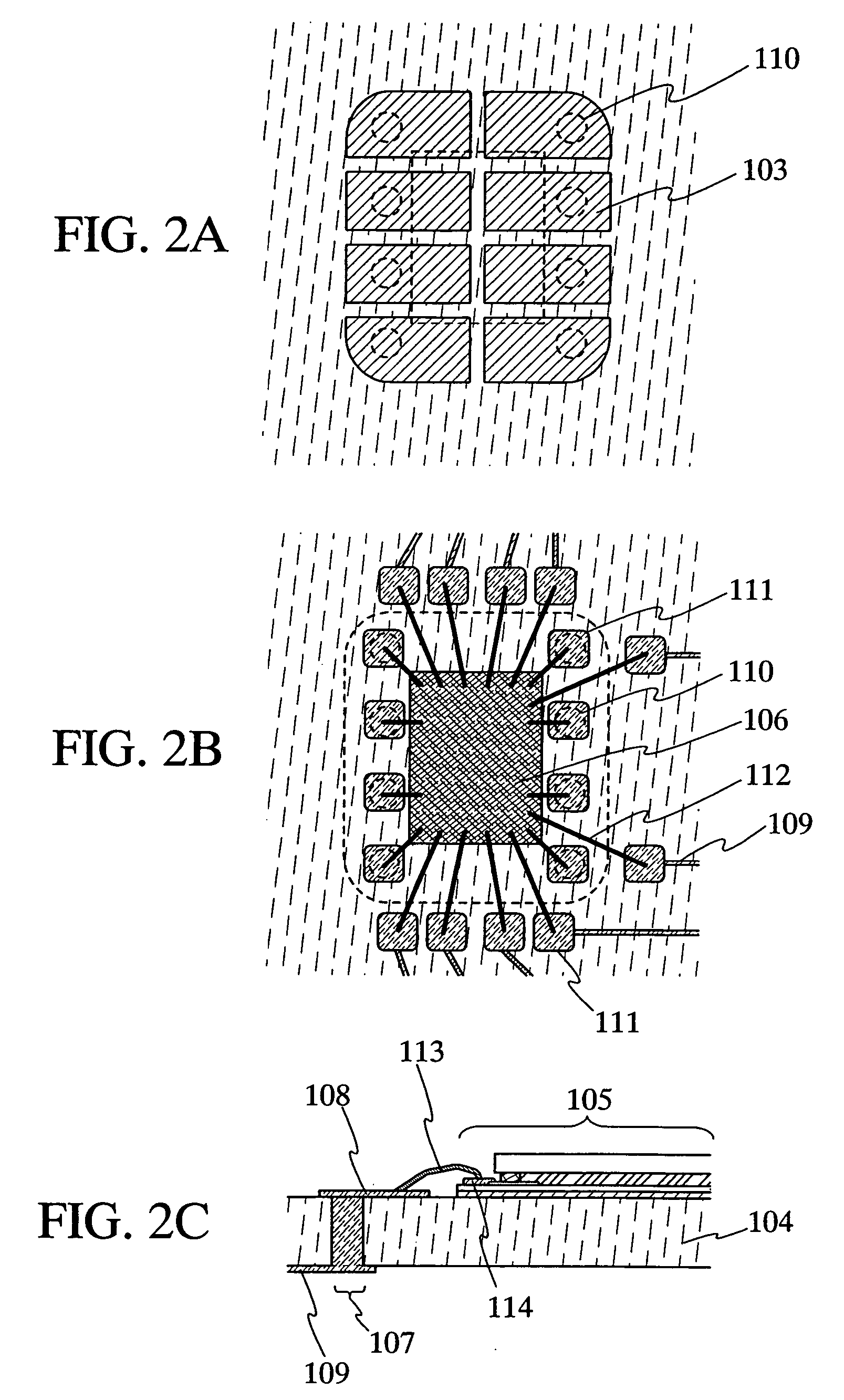
[0138] FIG. 11A is an oblique perspective figure showing a cross-sectional structure of the thin film integrated circuit connected to the interposer by a wire-bonding method. Reference number 601 denotes an interposer, 602 denotes a thin film integrated circuit. The thin film integrated circuit 602 is mounted over the interposer 601 by an adhesive agent 604 for mounting.

[0139] A connection terminal 605 is provided for a reverse side of the face over which the thin film integrated circuit 602 is mounted in the interposer 601 shown in FIG. 11A. A pad 606 provided for the interposer 601 is electrically connected to the connection terminal 605 via a contact hole provided for the interposer 601.

[0140] In this embodiment, the connection terminal 605 is electrically connected to the pad 606 directly through the contact...

embodiment 2

[0148] Embodiment 2

[0149] In this embodiment, a specific example of using an IC card of the present invention as an ATM card is described.

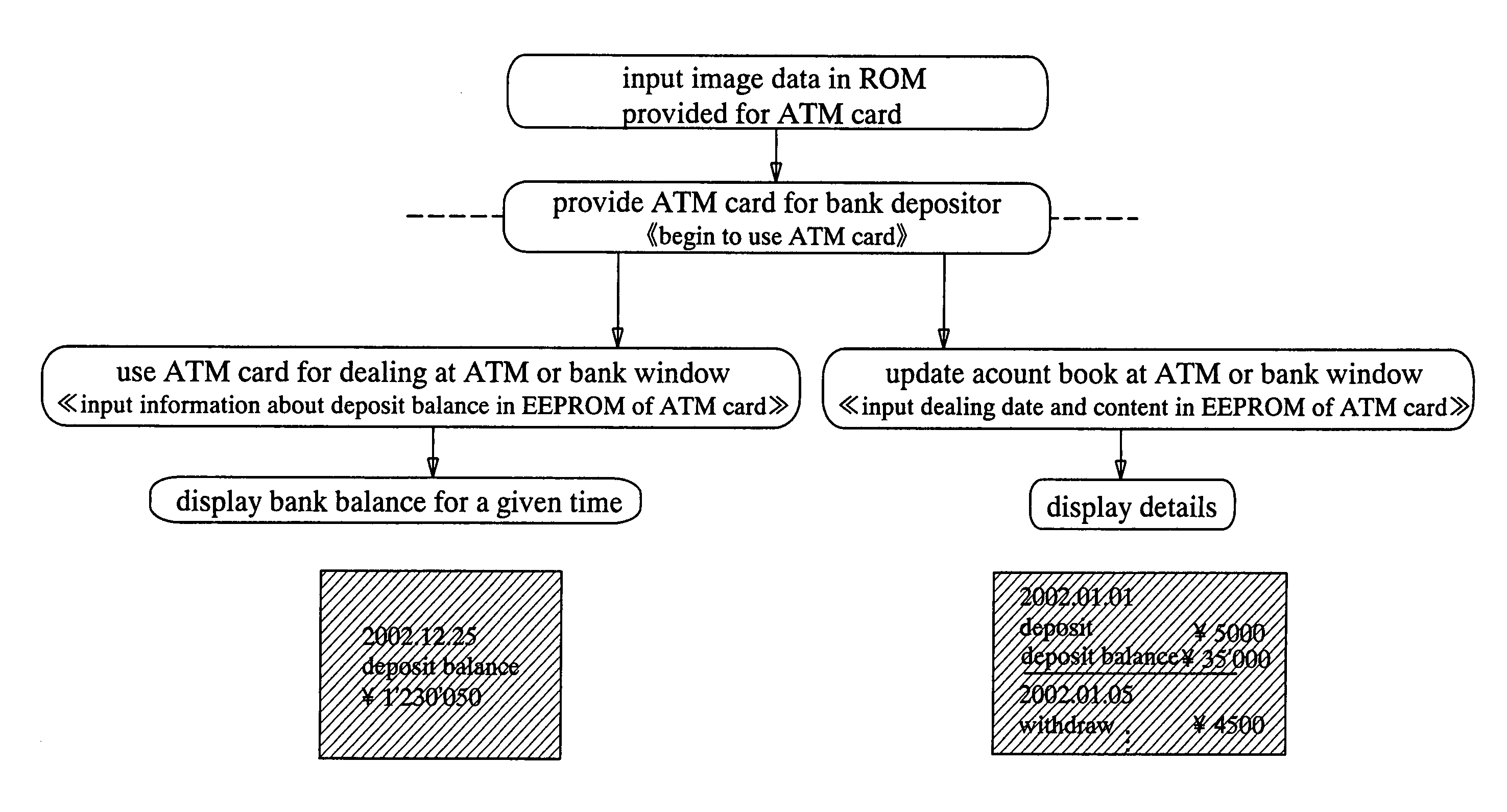
[0150] As shown in FIG. 12, image data of a bank depositor's face is memorized in a ROM provided for a thin film integrated circuit of an ATM card when he / she opens an account in a financial institution such as a bank. Forgery such as changing the photograph of a human face can be prevented by memorizing the data thereof in the ROM. The ATM card is provided for the bank depositor, and then he / she can begin to use the ATM card.

[0151] An ATM card is used for dealings at an ATM (automated teller machine) or a window. When dealing such as withdrawing, depositing, or transferring cash is done, details such as deposit balance or dealing date is required to be memorized in an EEPROM provided for a thin film integrated circuit of an ATM card.

[0152] After the dealing, details such as deposit balance or dealing date may be displayed in a pixel portion of th...

embodiment 3

[0155] Embodiment 3

[0156] In this embodiment, a case in which a plurality of liquid crystal display devices is manufactured from one substrate is described.

[0157] FIG. 13A is a top view of a substrate when a plurality of liquid crystal display devices is manufactured at the same time over a first substrate 1301. A sealing material 1302 to surround an area in which a liquid crystal is to be sealed is laid out and formed over the first substrate 1301 over which an alignment film is formed. A liquid crystal 1303 is dripped to the area surrounded by the sealing material 1302.

[0158] FIG. 13B is a cross sectional view along a broken line A-A' in FIG. 13A. As shown in FIG. 13B, the liquid crystal 1303 is dripped to the area surrounded by the sealing material 1302. Next, as shown in FIG. 13C, an opposite substrate 1304 is pressure-bonded so that the liquid crystal 1303 can be sealed within the area surrounded by the sealing material 1302.

[0159] After pressure-bonding the opposite substrate,...


PUM


Abstract

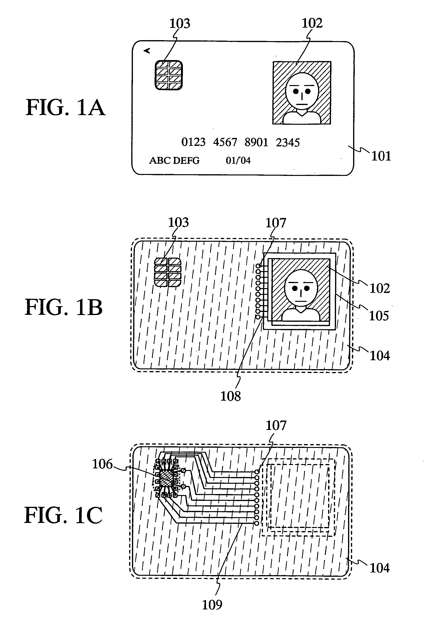
It is an object of the present invention to provide a highly sophisticated functional IC card that can ensure security by preventing forgery such as changing a picture of a face, and display other images as well as the picture of a face. An IC card comprising a display device and a plurality of thin film integrated circuits; wherein driving of the display device is controlled by the plurality of thin film integrated circuits; a semiconductor element used for the plurality of thin film integrated circuits and the display device is formed by using a polycrystalline semiconductor film; the plurality of thin film integrated circuits are laminated; the display device and the plurality of thin film integrated circuits are equipped for the same printed wiring board; and the IC card has a thickness of from 0.05 mm to 1 mm.

Description

[0001] 1. Field of the Invention[0002] The present invention relates to an IC card (which is also called a smart card) incorporating an integrated circuit such as a memory or a microprocessor (CPU). Further, the present invention relates to an booking-account system of a dealing content in the case of using the IC card as an ATM (automated teller machine) card (which is also called a cash card).[0003] 2. Description of the Related Art[0004] Several ten bytes of data only can be memorized in a magnetic card that can memorize data magnetically. However, an IC card incorporating a semiconductor memory, normally, can memorize about 5 KB of data or more. The IC card can assure much more capacity than a magnetic card. Further, the IC card has merits as follows: the IC card does not have a risk that data is read out by a physical means such as putting iron sand on a card, different from a magnetic card, and that data memorized in the IC card is not easily falsified.[0005] In recent years, ...

Claims


Application Information

Patent Timeline
IPC IPC(8): G06K19/077G07F7/10
CPCG06K19/077G06K19/07703H01L2224/73265H01L2224/48465H01L2224/48091H01L2924/10253G06Q20/105G06Q20/3415G07F7/1008H01L2924/01015H01L2924/01047H01L2924/3025H01L2224/45147H01L2924/00014H01L2924/00H01L2924/00011H01L2924/10271H01L2924/01005
Inventor TAKAYAMA, TORUMARUYAMA, JUNYAGOTO, YUUGOOHNO, YUMIKOAKIBA, MAI
Owner SEMICON ENERGY LAB CO LTD
Learn More