Method of improving stability in low k barrier layers

a barrier layer and stability technology, applied in the manufacture of cables/conductors, semiconductor/solid-state devices, coatings, etc., can solve the problems of short circuit formation, difficult etching of copper and achieving precise patterns, and failure of devices,

Inactive Publication Date: 2004-07-15
APPLIED MATERIALS INC
View PDF2 Cites 168 Cited by
  • Summary
  • Abstract
  • Description
  • Claims
  • Application Information

AI Technical Summary

Problems solved by technology

One difficulty in using copper in semiconductor devices is that copper is difficult to etch and achieve a precise pattern.
Etching with copper using traditional deposition/etch processes for forming interconnects has been less than satisfactory.
However, low k dielectric materials are often porous and susceptible to interlayer diffusion of conductive materials, such as copper, which can result in the formation of short-circuits and device failure.
This is unexpecte

Method used


Image

  • Method of improving stability in low k barrier layers
  • Method of improving stability in low k barrier layers
  • Method of improving stability in low k barrier layers

Examples


Embodiment Construction

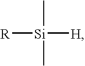
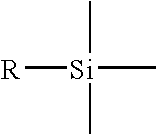
[0098] Organosilicon compounds described herein were deposited as barrier layers on substrate surface and analyzed. In one example, a silicon carbide film was deposited from a diphenylsilane compound and compared to a silicon carbide film from a conventional silicon carbide precursor, trimethylsilane.

[0099] Both diphenylsilane and trimethylsilane precursors were deposited by introducing diphenylsilane or trimethylsilane at about 500 mg / min into the processing chamber, introducing helium at about 500 sccm into the processing chamber, generating a plasma in the processing chamber by applying 100 watts of RF energy, maintaining the substrate temperature at about 290.degree. C., maintaining the chamber pressure at about 3 Torr to deposit a silicon carbide layer. The heater spacing was about 450 mils from the substrate surface.

[0100] The deposited films were examined and analyzed for dielectric constant and barrier layer diffusion. The diphenylsilane silicon carbide film had a measured d...


PUM

PropertyMeasurementUnit
Dielectric polarization enthalpyaaaaaaaaaa
Frequencyaaaaaaaaaa

Abstract

A method is provided for processing a substrate including providing a processing gas comprising hydrogen gas and an organosilicon compound comprising a phenyl group to the processing chamber, and reacting the processing gas to deposit a low k silicon carbide barrier layer useful as a barrier layer in damascene or dual damascene applications with low k dielectric materials.

Description

[0001] This application is related to U.S. patent application Ser. No. 10 / 010,950, filed Nov. 13, 2001, (Atty. Docket Number AMAT / 6392) and U.S. patent application Ser. No. 10 / 122,106, filed Apr. 11, 2002, (Atty. Docket Number AMAT / 6166), which are herein incorporated by reference to the extent not inconsistent with the disclosure and claims herein.BACKGROUND OF THE DISCLOSURE[0002] 1. Field of the Invention[0003] The invention relates to the fabrication of integrated circuits, more specifically to a process for depositing dielectric layers on a substrate, and to the structures formed by the dielectric layer.[0004] 2. Description of the Related Art[0005] Semiconductor device geometries have dramatically decreased in size since such devices were first introduced several decades ago. Since then, integrated circuits have generally followed the two year / half-size rule (often called Moore's Law), which means that the number of devices that will fit on a chip doubles every two years. Toda...

Claims


Application Information

Patent Timeline
IPC IPC(8): C23C16/32H01L21/314H01L21/768H01L23/532
CPCC23C16/325H01L21/3148H01L21/76801H01L21/7681H01L21/76825H01L23/53295H01L21/76828H01L21/76829H01L21/76835H01L23/5329H01L21/76826H01L2924/0002H01L21/02167H01L2924/00H01L21/02216H01L21/0234
Inventor LI, LIHUAHUANG, TZU-FANGXIA, LI-QUN
Owner APPLIED MATERIALS INC
Why Eureka
Try Eureka