Method of patterning magnetic products using chemical reaction

a magnetic product and chemical reaction technology, applied in the field of high-density magnetic recording technology, can solve the problems of reducing the quantity of magnetization per bit, limiting the resistance to thermal fluctuation, and loss of magnetization information

Inactive Publication Date: 2004-09-30
KK TOSHIBA
View PDF25 Cites 39 Cited by
  • Summary
  • Abstract
  • Description
  • Claims
  • Application Information

AI Technical Summary

Problems solved by technology

However, the minute recording bit reduces a quantity of magnetization per bit, and there arises a problem that is loss of magnetization information due to magnetization reversal by "thermal fluctuation".
However, if a density of the HDD is increased much more in the future, there may be a limit to resistance to thermal fluctuation even for the perpendicular magnetic recording mode.
However, since the magnetic material is hard to be etched unlike a general semiconductor material, it is difficult to use normal reactive ion etching (RIE) used in a semiconductor process.
However, in the above-described conventional manufacturing method, since the ferromagnetic material layer 520 is fabricated using the ion beam milling, damage remains on a crystal structure of the fabricated surface.
Thus, to carry, out fabrication of a good aspect ratio, a thin resist cannot be used.
However, there is a level difference of 20 to 50 nm attributable to presence / non-presence of a magnetic layer on the medium surface, and the level difference causes a problem of considerably reducing seeking durability.
However, these methods cannot completely remove the level difference on the medium surface.
In the case of using oxidation reaction, since a mask material having high resistance to oxidation should preferably be used, a normal resist removing step such as an O.sub.2 ashing process cannot be used to remove the mask material.
Consequently, the removing the mask material brings a process load.
However, short-circuiting may occur between the upper and lower ferromagnetic material layers because of etching damage or etching residuals.
On the other hand, the following problems exist concerning writing in the servo region formed in the magnetic recording medium.

Method used


Image

  • Method of patterning magnetic products using chemical reaction
  • Method of patterning magnetic products using chemical reaction
  • Method of patterning magnetic products using chemical reaction

Examples


first embodiment

[0052] [First Embodiment]

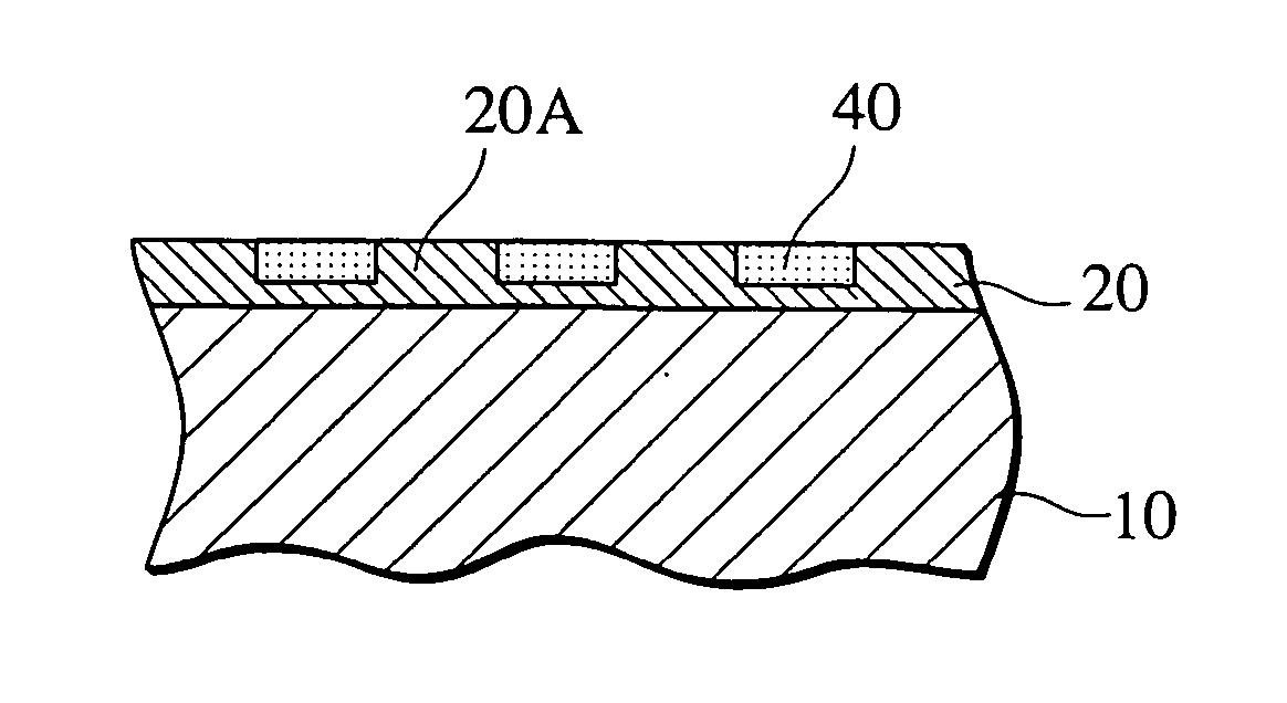
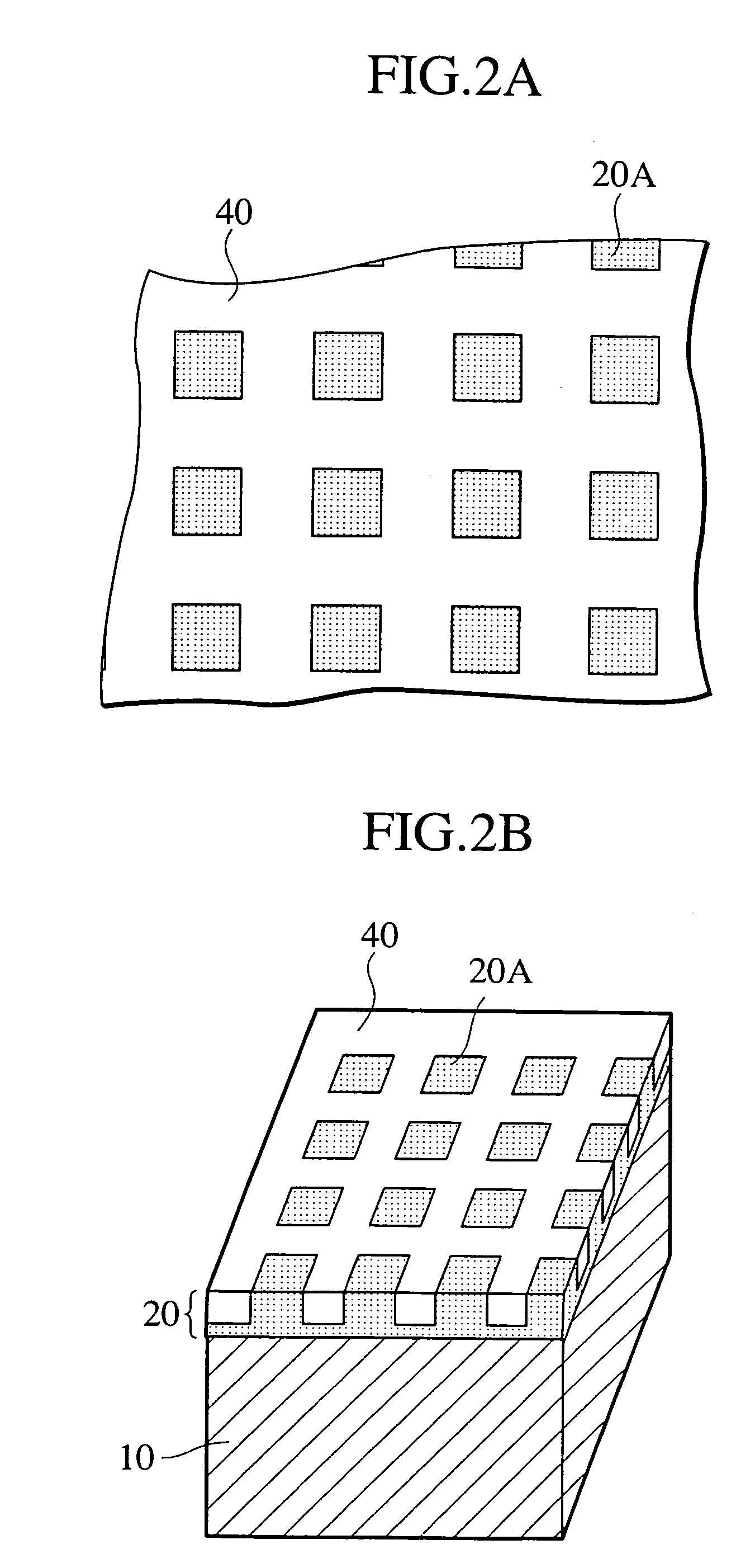
[0053] FIG. 2A is a partial plan view showing a structure of a magnetic recording medium according to a first embodiment of the present invention; and FIG. 2B is a perspective view of the same.

[0054] The magnetic recording medium of the first embodiment of the present invention is a so-called patterned medium. As shown in FIGS. 2A and 2B, this magnetic recording medium includes a recording layer 20 on a substrate 10. The recording layer 20 includes a ferromagnetic material region 20A and a nonferromagnetic material region 40. The ferromagnetic material region 20A contains any of Fe, Co and Ni, and has dotted exposed portions. The nonferromagnetic material region 40 surrounds at least an upper layer portion of the ferromagnetic material region 20A. Substantial recording regions are separated from each other by the nonferromagnetic material region 40. Here, the nonferromagnetic region means a region having lost magnetism at least as a ferromagnetic material, a...

example 2

[0093] (Example 2)

[0094] A patterned medium sample, in which ferromagnetic material CoPt regions are surrounded by antiferromagnetic material CoF.sub.2, was prepared. That is, first, CoPt was deposited by 20 nm on a Si substrate by a sputtering method. Then, resist was coated in a thickness of about 1.0 .mu.m on this CoPt film by spin coating, and a resist pattern as shown in FIG. 5A was formed after batch exposure and development. In this example, a size of each ferromagnetic material region on a surface layer was set to 2.0 .mu.m square.

[0095] A surface of this sample was exposed in F radicals generated under conditions similar to those of the example 1 for about 30 seconds while being maintained at room temperature. Then, the resist was removed by using an oxygen ashing apparatus.

[0096] When a MFM image of this sample was observed, a magnetic pattern equivalent to a resist pattern as shown in FIG. 5B was obtained. That is, regarding a region covered with a resist film, a MFM imag...

example 3

[0099] (Example 3)

[0100] In order to form finer patterns of the ferromagnetic material region than that of the above-described example 2, electron beam (EB) writing was carried out in exposure of resist. Accordingly, fine ferromagnetic material region patterns of about 80 nm square were formed. Other conditions were the same as those of the above example 2, and by using these conditions, a sample was prepared. That is, CoPt was deposited by 20 nm on a Si substrate by sputtering. Then, nega-resist was coated thereon, a minute resist pattern was formed by EB writing, and exposure thereof in F radicals was carried out for about 30 seconds at room temperature. Thereafter, the resist was removed.

[0101] An obtained sample was observed by MFM, and a single color image was obtained in a ferromagnetic material region. That is, it was verified that by reducing the ferromagnetic material region to a size of about 80 nm square, a single magnetic domain state was set in this region. When magneti...


PUM

PropertyMeasurementUnit
depthaaaaaaaaaa
thicknessaaaaaaaaaa
Neel temperaturesaaaaaaaaaa

Abstract

A method of patterning magnetic material includes forming a ferromagnetic material layer containing one element selected from the group consisting of Fe, Co and Ni on a substrate, selectively masking a surface of the ferromagnetic material layer, and making nonferromagnetic. The making nonferromagnetic step includes exposing an exposed portion in halogen-containing reaction gas, changing magnetism of the exposed portion and a lower layer thereof by chemical reaction, and making the exposed portion a nonferromagnetic material region. A magnetic recording medium is fabricated by using the magnetic material patterning method and includes a plurality of recording regions made of ferromagnetic materials, each containing at least one element selected from the group consisting of Fe, Co and Ni, and a nonferromagnetic material region for separating the recording regions from each other. The nonferromagnetic material region is a compound region of the ferromagnetic material and halogen.

Description

[0001] This application is based upon and claims the benefit of priority from the prior Japanese Patent Applications No. 2001-102215 filed on Mar. 30, 2001 and No. 2001-399848 filed on Dec. 28, 2001, the entire contents of which are incorporated herein by reference.[0002] 1. Field of the Invention[0003] The present invention relates to a high-density magnetic recording technology and, more particularly, to a method of patterning magnetic products, magnetic recording media such as patterned media produced by this method, and other magnetic products, and to a magnetic recording apparatus equipped with such magnetic recording media.[0004] 2. Description of the Related Art[0005] In recent years, because of an increase in a surface recording density of a magnetic recording medium along with an increased recording capacity of a hard disk drive (referred to as HDD, hereinafter), each recording bit size on the magnetic recording medium has become extremely minute, about several 10 nm. To ob...

Claims


Application Information

Patent Timeline
Patent Type & Authority Applications(United States)
IPC IPC(8): G11B5/00G11B5/64G11B5/48G11B5/58G11B5/596G11B5/65G11B5/74G11B5/82G11B5/84G11B5/855G11B9/00H01F10/16H01F41/34H01L21/8246H01L27/105H01L43/08
CPCB82Y10/00Y10T428/12465G11B5/488G11B5/58G11B5/596G11B5/74G11B5/743G11B5/82G11B5/855G11B9/1418G11B2005/0002G11B2005/0005Y10T428/31Y10T428/24479Y10T428/25G11B5/00H10N50/01
Inventor KAMATA, YOSHIYUKINAITO, KATSUYUKIHIEDA, HIROYUKI
Owner KK TOSHIBA
Why Eureka
Try Eureka