

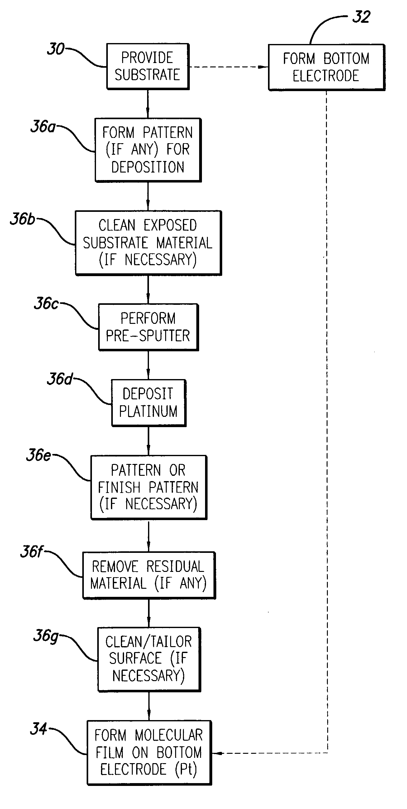
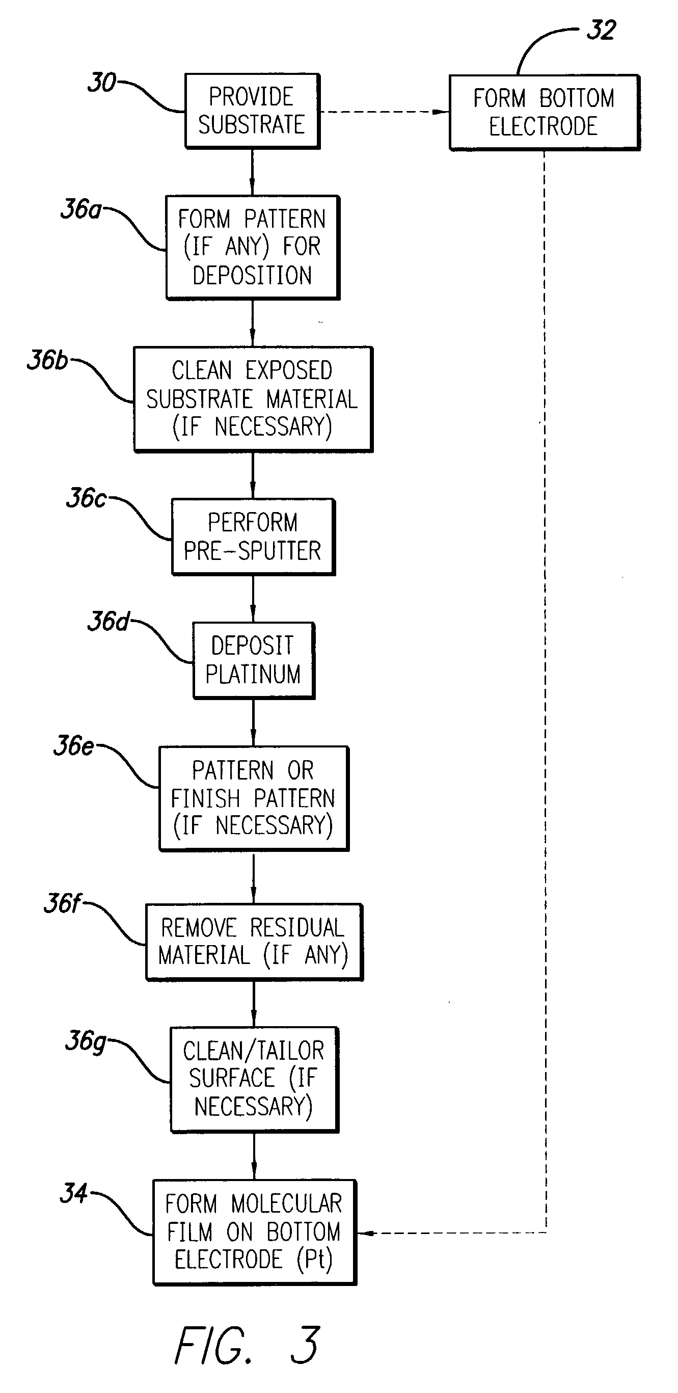
Custom electrodes for molecular memory and logic devices
a logic device and molecular memory technology, applied in the field of custom electrodes for molecular memory and logic devices, can solve the problems of decreasing the number of electrons either accessed or utilized within the device, becoming increasingly difficult to design well-behaved devices, and increasing the difficulty of fabrication and cost. achieve the effect of low surface roughness
- Summary
- Abstract
- Description
- Claims
- Application Information
AI Technical Summary
Benefits of technology
Problems solved by technology
Method used
Image

Examples
examples
[0089] Experimental Procedure
[0090] Both the blanket and photolithographically-modified Pt films were sputter deposited on Si wafers with a 100 nm silicon dioxide layer. The typical Pt thickness was 100 nm. The plasma treatment was performed in a RIE.RTM. model 1700 system. Freshly deposited Pt films and films exposed to various plasma treatments were analyzed with contact angle and ellipsometry measurements within 10 minutes of preparation and by XPS and Auger with controls.
[0091] For contact angle measurements a droplet of 2 .mu.L 18 M.OMEGA..multidot.cm water was injected onto the sample surface from a syringe. An image of the static water droplet was recorded with a digital camera and analyzed to yield a sessile contact angle, averaging at least three readings.
[0092] Ellipsometric measurements were performed using a laser with a wavelength of 532 nm and an incident angle of 58 degrees. A simple model was used to derive the optical constants, n and k. The platinum was approximate...
PUM
 Abstract
Description
Claims
Application Information