Method of manufacturing potassium niobate single crystal thin film, surface acoustic wave element, frequency filter, frequency oscillator, electric circuit, and electronic apparatus

a technology of potassium niobate and single crystal thin film, applied in the direction of polycrystalline material growth, device material selection, natural mineral layered products, etc., can solve the problems of low k.sup.2, low k.sup.2, and low k.sup.2, and achieve the effect of reducing the number of acoustic waves

Inactive Publication Date: 2004-10-07
SEIKO EPSON CORP
View PDF9 Cites 61 Cited by
  • Summary
  • Abstract
  • Description
  • Claims
  • Application Information

AI Technical Summary

Problems solved by technology

In addition, the propagation velocity is slow in comparison to SrTiO.sub.3 and CaTiO.sub.3, which are also perovskite-type oxides.
Thus, when only a KNbO.sub.3 single crystal substrate is used, the sound velocity, high k.sup.2, and zero temperature properties cannot all be satisfied.
However, the surface acoustic wave element using these KNbO.sub.3 piezoelectric thin films have the following problems.
Thus, there is the problem that in comparison to the starting composition, the composition of the thin film after manufacture deviates towards the Nb excess side.

Method used


Image

  • Method of manufacturing potassium niobate single crystal thin film, surface acoustic wave element, frequency filter, frequency oscillator, electric circuit, and electronic apparatus
  • Method of manufacturing potassium niobate single crystal thin film, surface acoustic wave element, frequency filter, frequency oscillator, electric circuit, and electronic apparatus
  • Method of manufacturing potassium niobate single crystal thin film, surface acoustic wave element, frequency filter, frequency oscillator, electric circuit, and electronic apparatus

Examples


first embodiment

[0082] First Embodiment of the Surface Acoustic Wave Element

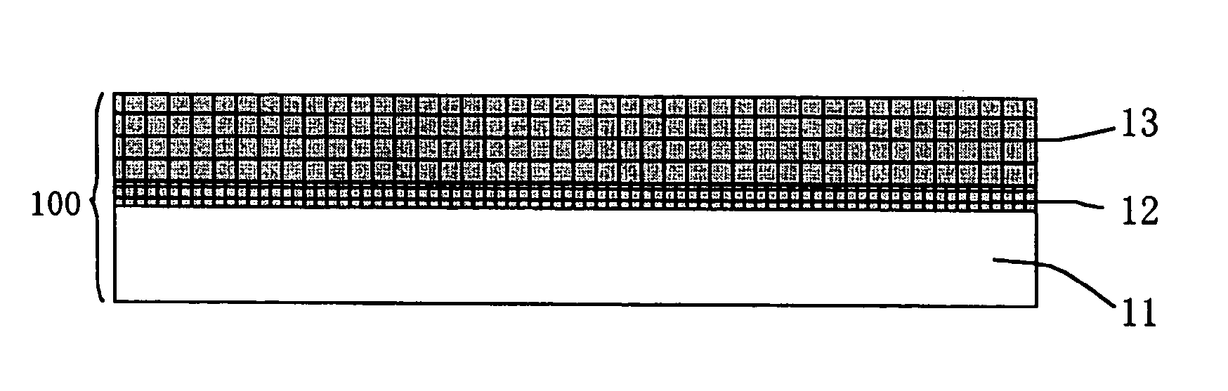
[0083] FIG. 7 is a cross-sectional drawing showing the first embodiment of the surface acoustic wave element of the present invention.

[0084] First, by vacuum deposition using metal aluminum, at a substrate temperature of 25.degree. C., and a vacuum of 5.times.10.sup.-7 Torr, a 100 nm Al electrode 17 was deposited on the KNbO.sub.3 single crystal layer 13. Note that the substrate temperature, and the vacuum degree are not limited thereby.

[0085] Next, a continuous process of patterning using a resist application, light exposure, dry etching, and resist removal was carried out on the Al electrode 17, and the IDT electrodes 18 and 19 were formed on the KNbO.sub.3 single crystal layer 13.

[0086] The sound velocity of the obtained surface acoustic wave element found from the delay time V.sub.open of the surface acoustic wave between the IDT electrodes 18 and 19 was 4000 m / s. From the difference between the delay time V.sub.open an...

second embodiment

[0107] Second Embodiment of the Surface Acoustic Wave Element

[0108] FIG. 9 is a cross-sectional diagram showing the second embodiment of the surface acoustic wave element of the present invention.

[0109] IDT electrodes 18 and 19 are formed on the KNbO.sub.3 single crystal layer 27 completely identically to the first embodiment of the surface acoustic wave element.

[0110] The sound velocity of the obtained surface acoustic wave element found from the delay time V.sub.open of the surface acoustic wave between the IDT electrodes 18 and 19 was 5000 m / s. From the difference between the delay time V.sub.open and the delay time V.sub.short of the surface acoustic wave when a metal thin film covered the gap between the IDT electrodes 18 and 19, k.sup.2 was 20%. In the case that the KNbO.sub.3 single crystal thin film manufacture was not carried out, the sound velocity was the same 5000 m / s, but k.sup.2 became a low 8%, and it is clear that k.sup.2 was improved by making the KNbO.sub.3 thin fi...

third embodiment

[0128] Third Embodiment of the Surface Acoustic Wave Element

[0129] FIG. 11 is a cross-sectional drawing of the third embodiment of the surface acoustic wave element of the present invention.

[0130] IDT electrodes 18 and 19 are formed on the KNbO.sub.3 single crystal layer 35 completely identically to the first embodiment of the surface acoustic wave element.

[0131] The sound velocity of the obtained surface acoustic wave element found from the delay time V.sub.open of the surface acoustic wave between the IDT electrodes 18 and 19 was 3000 m / s. From the difference between the delay time V.sub.open and the delay time V.sub.short of the surface acoustic wave when a metal thin film covered the gap between the IDT electrodes 18 and 19, k.sup.2 was 15%. In the case that the KNbO.sub.3 single crystal thin film manufacture was not carried out, the sound velocity was the same 3000 m / s, but k.sup.2 became a low 5%, and it is clear that k.sup.2 was improved by making the KNbO.sub.3 thin film a s...


PUM

PropertyMeasurementUnit
melting pointaaaaaaaaaa
eutectic temperatureaaaaaaaaaa
temperatureaaaaaaaaaa

Abstract

A method of manufacturing a potassium niobate (KNbO3) single crystal thin film, includes the steps of maintaining the substrate under a predetermined oxygen partial pressure; maintaining the substrate within a temperature region which is equal to or higher than an eutectic temperature of KNbO3 and 3K2O.Nb2O5 and is equal to or lower than complete melting temperature of KNbO3 and 3K2O.Nb2O5 so that a solid phase of KNbO3 and a liquid phase can coexist on the substrate; depositing a vapor phase material on the substrate in a state in which a solid phase and a liquid phase coexist; and precipitating KNbO3 on the substrate from the liquid phase as a solid phase to grow a KNbO3 single crystal thin film. The composition of a starting material to be vaporized to generate the vapor phase material is from K2O.Nb2O5=50:50 to K2O.Nb2O5=65:35.

Description

[0001] 1. Field of the Invention[0002] The present invention relates to a surface acoustic wave element used in telecommunication devices, and in particular relates to a surface acoustic wave element that uses a piezoelectric thin film.[0003] 2. Description of the Related Art[0004] There has been a remarkable expansion in the demand for surface acoustic wave elements with the rapid developments in the telecommunication field centered on mobile communication, which is typified by mobile telephones. Some trends in the development of surface acoustic wave elements include size reduction, increasing efficiency, and increasingly higher frequencies. In order to attain these, a larger electromechanical coupling coefficient (below, k.sup.2), more stable temperature characteristics, and a higher surface acoustic wave propagation velocity become necessary. For example, when used as a high frequency filter, a high k.sup.2 is desirable in order to obtain a pass band having a small loss and a wi...

Claims


Application Information

Patent Timeline
Patent Type & Authority Applications(United States)
IPC IPC(8): C30B19/00C30B29/30H01L41/09H01L41/18H01L41/311H01L41/316H01L41/317H01L41/39H03B5/30H03H3/08H03H9/02H03H9/25
CPCC30B19/00H03H3/08H03H9/02574C30B29/30
Inventor HIGUCHI, TAKAMITSUIWASHITA, SETSUYAMIYAZAWA, HIROMU
Owner SEIKO EPSON CORP
Why Eureka
Try Eureka