Activation plate for electroless and immersion plating of integrated circuits

a technology of active plate and integrated circuit, which is applied in the direction of metallic material coating process, surface reaction electrolytic coating, solid-state device, etc., can solve the problems of deterioration of the pad, performance degradation and product failure, and easy corrosion of the aluminum bond pad on the integrated circuit under standard environmental test conditions

Inactive Publication Date: 2005-01-06
TAIWAN SEMICON MFG CO LTD
View PDF3 Cites 39 Cited by
  • Summary
  • Abstract
  • Description
  • Claims
  • Application Information

AI Technical Summary

Problems solved by technology

Aluminum wirebonds well, yet aluminum bond pads on integrated circuits are susceptible to corrosion under standard environmental test conditions.
This corrosion can cause performance degradation and product failure when the joint between the gold wire and aluminum pad degrades and fails.
These methods for gold and nickel-phosphorous, however, run the risk, like other processes using multiple layers, of creating a mushrooming effect over passivation layers and consequential shorting between pads in fine-pitch arrays.
Difficulties in such a process still include creating a uniform bonding surface with no nodules or foreign matter.
Copper, however, is susceptible to corrosion, and is not easily soldered or wire-bonded.
Unfortunately, dispensing and curing the silicone is a time-consuming process.
The silicone, having a higher dielectric constant and loss tangent than air, may cause a degradation of high-frequency and RF performance.
In addition, it is difficult to remove the silicone compound completely, precluding rework and repair.
This partial solution, however, is limited because many die in the RF section and most of the die in the digital section of an assembly have aluminum bond pads, and therefore must still be encapsulated with the silicone compound for corrosion resistance.
These problems cause some pads on an integrated circuit or semiconductor wafer to plate differently than others.
This uniformity and consistency is difficult to obtain when bond pads are of different sizes, different locations, and different metallurgies, and have different connectivities to the underlying semiconductor substrate, which result in small yet impactive electric potentials that vary from pad to pad.
Other issues may cause plating problems, such as varying pad metal composition, bond pad porosity, grain boundaries, variations in the surface finish of the pad metal, and thin pad metal.
Other potential issues include inadequate passivation coverage, nodule formation, poor plating on pads grounded to the silicon substrate, galvanic cell effects that interrupt the plating process, photovoltaic effects that produce voltages at p-n junctions affecting the plating on associated bond pads, loss of plated material, inadequate coverage, local inhibition of the plating process, and overly aggressive cleaning cycles.

Method used


Image

  • Activation plate for electroless and immersion plating of integrated circuits
  • Activation plate for electroless and immersion plating of integrated circuits
  • Activation plate for electroless and immersion plating of integrated circuits

Examples


Embodiment Construction

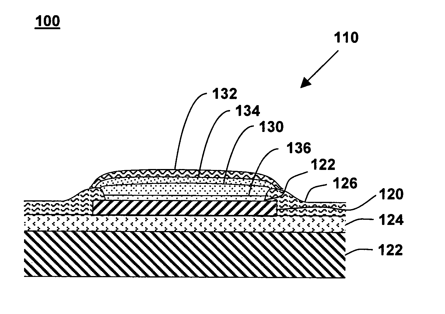
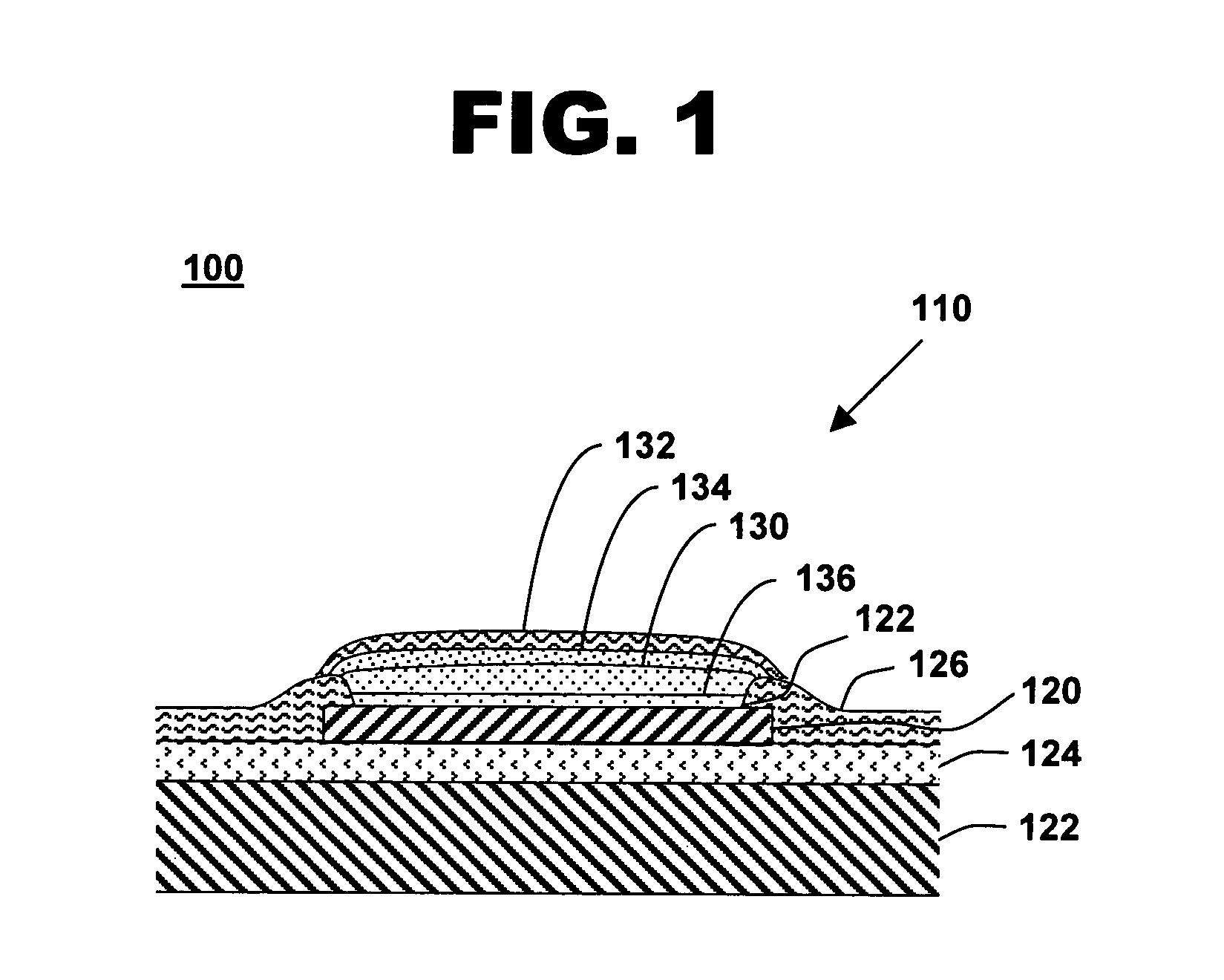
[0023]FIG. 1 shows a cross-sectional cutaway view of a plated bond pad on an integrated circuit, in accordance with one embodiment of the present invention at 100. Multiple bond pads 120 are typically located on the surface of an integrated circuit 110. The bond pads provide for electrical connections such as external power supplies, ground lines, input signals, output signals, data lines, address lines, other integrated circuits, and external electronic components. Integrated circuit 110 includes a plurality of bond pads 120. Integrated circuit 110 with the plurality of bond pads 120 may be contained, for example, on an undiced semiconductor wafer or on an individual semiconductor die.

[0024] Bond pad 120 is electrically isolated from a semiconductor substrate 122 such as a silicon substrate by one or more insulating layers 124. Insulating layer 124 may comprise, for example, a layer of silicon dioxide or silicon nitride. A passivation layer 126 typically covers the majority of the...


PUM

PropertyMeasurementUnit
distanceaaaaaaaaaa
distanceaaaaaaaaaa
thicknessaaaaaaaaaa

Abstract

The invention provides a method of plating an integrated circuit. An activation plate is positioned adjacent to at least one integrated circuit. The integrated circuit includes a plurality of bond pads comprising a bond-pad metal, and the activation plate also comprises the bond-pad metal. A layer of electroless nickel is plated on the bond pads and the activation plate, and a layer of gold is plated over the layer of electroless nickel on the bond pads and the activation plate. An integrated circuit with bond pads plated using the activation plate, and a system for plating an integrated circuit is also disclosed.

Description

FIELD OF THE INVENTION [0001] The invention relates generally to semiconductor processing. More particularly, the invention relates to a method for plating metal bond pads on an integrated circuit using electroless and immersion plating. BACKGROUND OF THE INVENTION [0002] In the electronics industry, electroless plating and immersion plating are widely used processes for applying metal coatings to substrates. The processes are used extensively, for example, in printed circuit board and integrated package interposer fabrication, and in plating solderable or wirebondable finishes such as nickel-gold to copper surface pads. Electroless and immersion plating have been used to improve bond-pad properties for packaging where the integrated circuit interconnect metal is unacceptable. [0003] Aluminum, for example, is not solderable, although an electroless nickel and immersion gold under-bump metallurgy (UBM) on aluminum bond pads provides solderability for flip-chip assemblies. Aluminum wi...

Claims


Application Information

Patent Timeline
Patent Type & Authority Applications(United States)
IPC IPC(8): C23C18/16C25D11/18H01L21/302H01L21/44H05K3/24
CPCC23C18/1651H05K2201/10204H05K3/244H01L24/03H01L24/05H01L2224/03464H01L2224/0401H01L2224/04042H01L2224/05644H01L2224/45124H01L2224/45144H01L2224/94H01L2924/14H01L2224/03H01L2924/00
Inventor DEAN, TIMOTHY B.LYTLE, WILLIAM H.
Owner TAIWAN SEMICON MFG CO LTD
Why Eureka
Try Eureka