Photomask blank substrate, photomask blank and photomask

a technology of substrate and photomask, which is applied in the direction of photomechanical treatment, instruments, chemistry apparatus and processes, etc., can solve the problems of inability to ignore the flatness of the substrate as a cause of focal shift, the number of technical challenges concerning the accuracy of photolithographic processes employed in semiconductor manufacturing, etc. achieve good surface flatness, accurate alignment, and high flatness

Active Publication Date: 2005-01-27
SHIN ETSU CHEM IND CO LTD +2
View PDF6 Cites 44 Cited by
  • Summary
  • Abstract
  • Description
  • Claims
  • Application Information

AI Technical Summary

Benefits of technology

[0019] The substrates of the invention exhibit a good surface flatness when used as photomasks, that is, at the time of wafer exposure. When a photomask fabricated from a photomask blank obtained from such a substrate is held on the mask stage of a wafer exposure system with a vacuum chuck or the like, the substrate surface undergoes minimal warping. Hence, the photomask has a high flatness. Because the mask pattern can be accurately aligned at a predetermined position, exposure patterns of small minimum feature size can be written onto wafers to good position and linewidth accuracies, thus making it possible to fully satisfy requirements for smaller pattern geometries in photolithography.

Problems solved by technology

These trends have led to a number of technical challenges concerning the accuracy of photolithographic processes employed in semiconductor manufacturing.
One such challenge relates to the flatness of the photomask used in lithography.
As the minimum feature size becomes smaller, the focal depth allowed by the resist becomes smaller, making it impossible to disregard the flatness of the substrate as a cause of focal shift.
Nor has anything been known about what sort of method may be used to form such a surface shape so as to enable the production of substrates having the desired surface shape in a good yield or about how to suppress the formation of defects on the substrate itself or of photomask defects that originate from the substrate.

Method used


Image

  • Photomask blank substrate, photomask blank and photomask
  • Photomask blank substrate, photomask blank and photomask
  • Photomask blank substrate, photomask blank and photomask

Examples


first embodiment

[0035] The photomask blank substrate in the first embodiment of the invention is described.

[0036] The photomask blank substrate in the first embodiment is a substrate which is quadrangular and has a length on each side of at least 6 inches. The substrate has a top surface on which a mask pattern is to be formed. A pair of strip-like regions extend from 2 to 10 mm inside each of a pair of opposing sides along an outer periphery of the substrate top surface, with a 2 mm edge portion excluded at each end in a lengthwise direction thereof. Each of the strip-like regions is inclined downward toward the outer periphery of the substrate. A difference between maximum and minimum values for height from a least squares plane for the strip-like regions on the substrate top surface to the strip-like regions themselves is at most 0.5 μm.

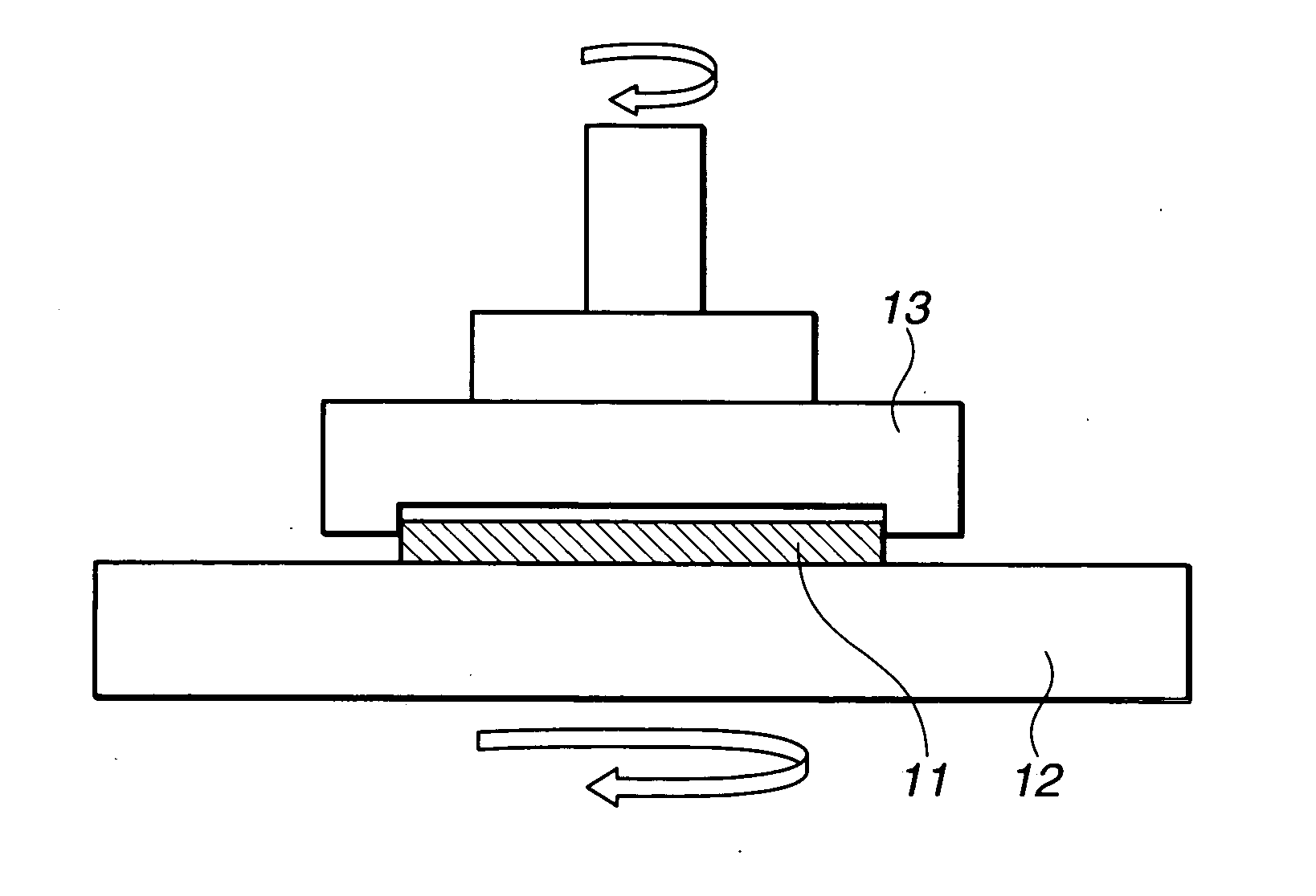
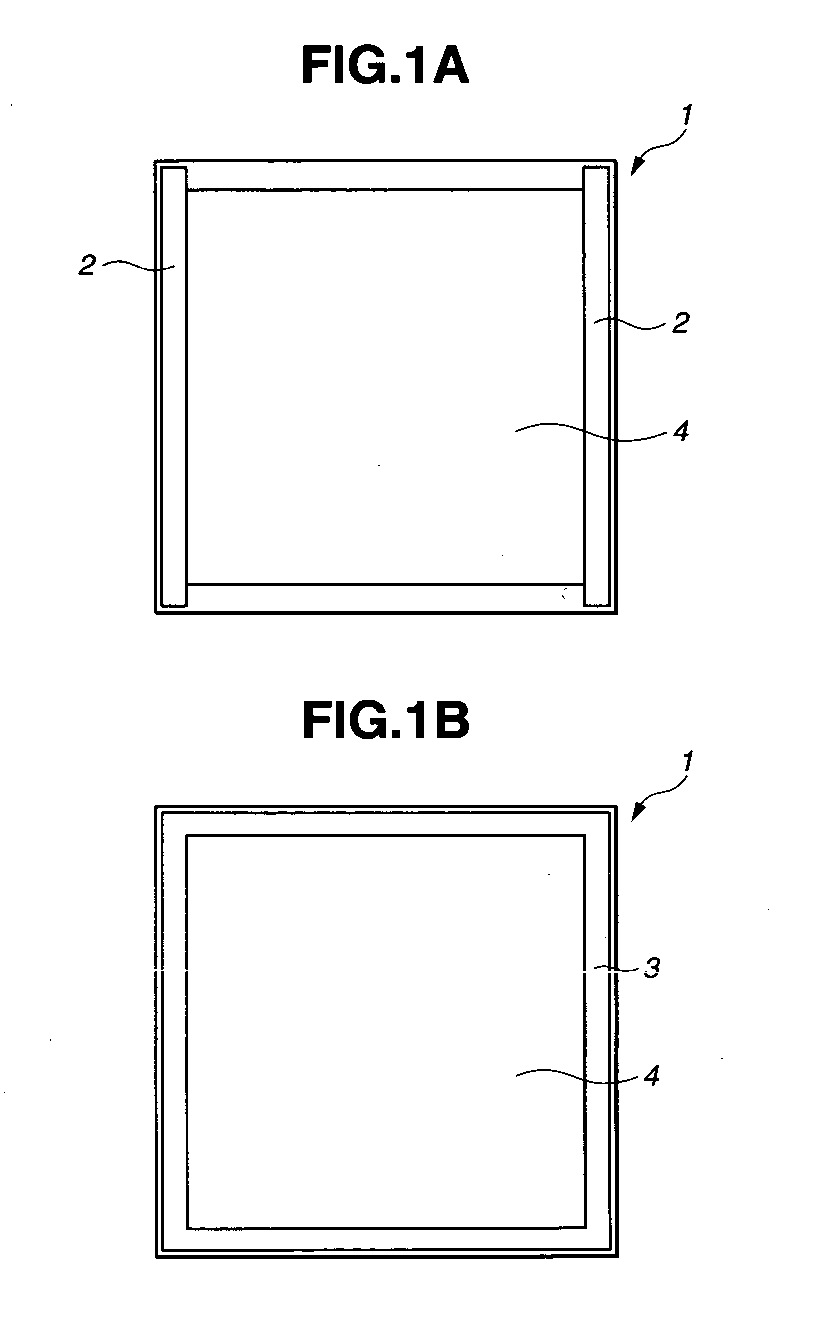
[0037] The term “strip-like region” as used herein is explained below while referring to FIG. 1A, which shows the substrate top surface 1 on which a suitable f...

second embodiment

[0041] The photomask blank substrate in the second embodiment of the invention is described.

[0042] The photomask blank substrate in the second embodiment is a substrate which is quadrangular and has a length on each side of at least 6 inches. The substrate has a top surface on which a mask pattern is to be formed. A quadrangular ring-shaped region extends from 2 to 10 mm within each side along an outer periphery of the substrate top surface. The quadrangular ring-shaped region is inclined downward toward the outer periphery of the substrate. A difference between maximum and minimum values for height from a least squares plane for the quadrangular ring-shaped region on the substrate top surface to the quadrangular ring-shaped region itself is at most 0.5 μm.

[0043] The term “quadrangular ring-shaped region” as used herein is explained below while referring to FIG. 1B, which shows the substrate top surface 1 on which a suitable film such as a film having light-shielding properties, o...

third embodiments

[0050] The photomask blank substrate in the third embodiment of the invention is described.

[0051] The photomask blank substrate in the third embodiment is a substrate which is quadrangular and has a length on each side of at least 6 inches. The substrate has a top surface on which a mask pattern is to be formed. A quadrangular ring-shaped region extends from 2 to 10 mm within each side along an outer periphery of the substrate top surface. When a least squares plane for the quadrangular ring-shaped region on the substrate top surface is considered a reference plane, and a circle having a center at the center of the substrate is drawn on the reference plane so as to traverse the reference plane, a difference between maximum and minimum values for height from the reference plane to the quadrangular ring-shaped region, taken in an arcuate portion passing the reference plane, is at most 0.3 μm.

[0052] The term “quadrangular ring-shaped region” as used herein is explained below while re...


PUM

PropertyMeasurementUnit
heightaaaaaaaaaa
heightaaaaaaaaaa
lengthaaaaaaaaaa

Abstract

In a quadrangular photomask blank substrate with a length on each side of at least 6 inches, which has a pair of strip-like regions that extend from 2 to 10 mm inside each of a pair of opposing sides along an outer periphery of a substrate top surface, with a 2 mm edge portion excluded at each end, each strip-like region is inclined downward toward the outer periphery of the substrate, and a difference between maximum and minimum values for height from a least squares plane for the strip-like region to the strip-like region is at most 0.5 μm. The substrate exhibits a good surface flatness at the time of wafer exposure.

Description

CROSS-REFERENCE TO RELATED APPLICATION [0001] This Nonprovisional application claims priority under 35 U.S.C. §119(a) on Patent Application Nos. 2003-280437 and 2003-280462 filed in Japan on Jul. 25, 2003 and Jul. 25, 2003, respectively, the entire contents of which are hereby incorporated by reference.BACKGROUND OF THE INVENTION [0002] 1. Field of the Invention [0003] The present invention relates to substrates for photomask blanks from which photomasks can be fabricated for use in photolithography associated with the manufacture of semiconductor devices and related products. It also relates to photomask blanks and photomasks prepared therefrom. [0004] 2. Prior Art [0005] As semiconductor devices continue to become more highly integrated, there is a growing desire for smaller geometries in photolithography. Already, the design rule for devices has been lowered to 0.11 μm and patterns are required to be accurate to 10 nm or less. These trends have led to a number of technical challe...

Claims


Application Information

Patent Timeline
Patent Type & Authority Applications(United States)
IPC IPC(8): B32B9/00B32B17/06G03F1/00G03F1/60G03F9/00
CPCG03F1/60G03F1/14G03F1/50
Inventor NAKATSU, MASAYUKINUMANAMI, TSUNEOMOGI, MASAYUKIITOH, MASAMITSUHAGIWARA, TSUNEYUKIKONDO, NAOTO
Owner SHIN ETSU CHEM IND CO LTD
Why Eureka
Try Eureka