

Method and apparatus for forming a ferroelectric layer
a ferroelectric layer and crystalline structure technology, applied in the direction of coatings, solid-state devices, chemical vapor deposition coatings, etc., can solve the problems of capacitor located on buried contact plugs, pt/iro/ir electrodes, capacitors may degrade, etc., to improve the crystalline structure of the ferroelectric layer
- Summary
- Abstract
- Description
- Claims
- Application Information
AI Technical Summary
Benefits of technology
Problems solved by technology
Method used
Image

Examples
Embodiment Construction
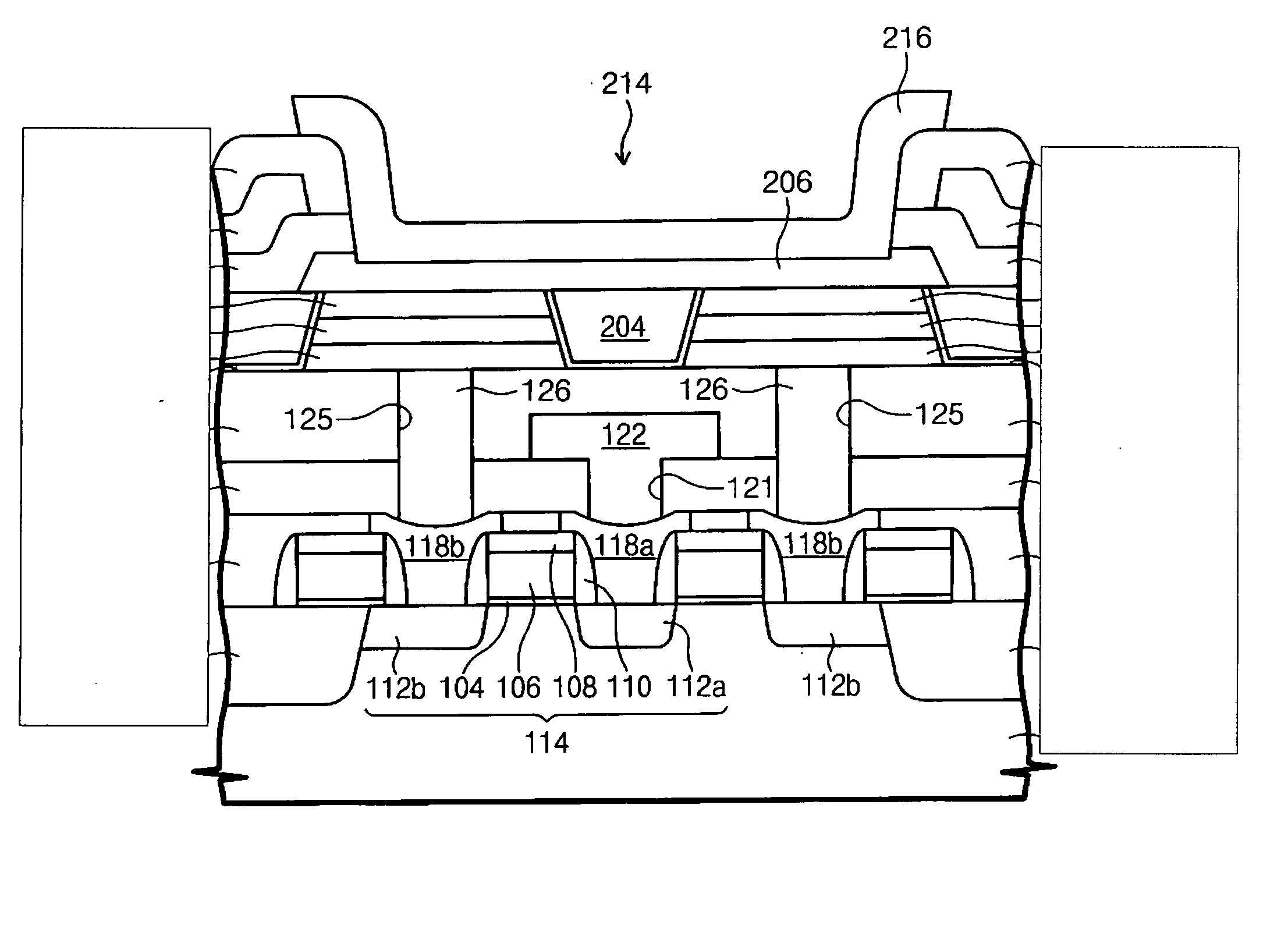
[0077]FIG. 14 illustrates an apparatus in accordance with an exemplary embodiment of the present invention. As shown in FIG. 14, the apparatus may include a process chamber 500, a susceptor 510, a showerhead 520, a first gas injection part 540, a second gas injection part 560, and a purge gas injection part 570. The showerhead 520 may further include a first injection part 520a and a second injection part 520b. The first injection part 540 may include a vaporizer 530 which receives a carrier gas and a liquid metal organic source and vaporizes the combination and a valve 542 may supply the mixed vaporized gas to the showerhead 520. The second gas injection part 560 may include an external heater 550 for receiving a gas, such as oxygen gas and a valve 562 for controlling the flow of heated oxygen gas to the second injection part 520b of the showerhead 520. The purge gas injection 570 may include a valve 572 for controlling the flow of purged gas to the first injection part 520a of the...
PUM
| Property | Measurement | Unit |
|---|---|---|
| Temperature | aaaaa | aaaaa |
| Temperature | aaaaa | aaaaa |
| Temperature | aaaaa | aaaaa |
Abstract
Description
Claims
Application Information