Single-transverse-mode VCSEL device with array structure and fabrication method thereof
- Summary
- Abstract
- Description
- Claims
- Application Information
AI Technical Summary
Benefits of technology
Problems solved by technology
Method used
Image

Examples
first embodiment
[0026] The first embodiment is given to explain the basic grain structure of the single-transverse-mode VCSEL device and the fabrication method thereof.
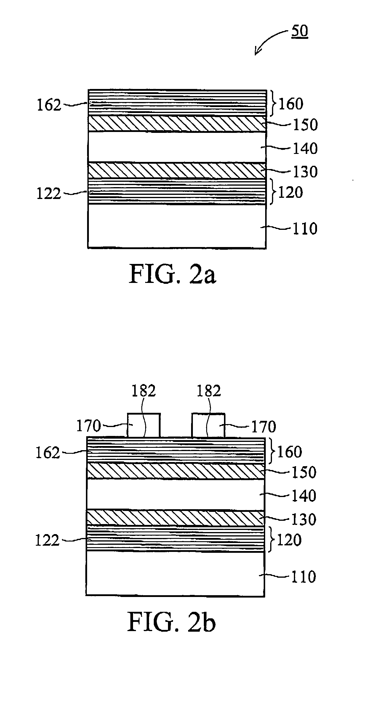
[0027]FIG. 2a shows the cross-section of the basic grain structure of the single-transverse-mode VCSEL device.
[0028] The grain 50 includes a semiconductor substrate 110, a first-type DBR 120, a first-type cladding layer 130, an active layer 140, a second-type cladding layer 150 and a second-type OBR 160. The fabrication method is described as follows.
[0029] First, a semiconductor substrate 110 is provided. A first-type DBR 120 is then formed on the semiconductor substrate 110. The semiconductor substrate 110 can be made of As, Al, Ga, In, Sb, Se, Ti, or Si, or a nitride, oxide, fluoride or a compound comprising at least one of the above elements. In this case, the semiconductor substrate 110 is an GaAs substrate. The first-type DSR 120 is mainly a stack of alternating layers of two different first-type layers 122, wherein the numb...
second embodiment
[0033] The second embodiment is taken to explain the fabrication method of the inventive single-transverse-mode VCSEL device with array structure.
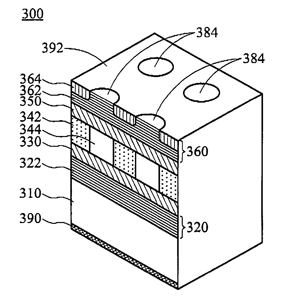
[0034]FIGS. 2a-2f illustrate the fabrication process of the inventive single-transverse-mode VCSEL device with array structure, and FIG. 3 is a cross-section of a single-transverse-mode VCSEL device with a 2×1 array structure in the embodiment.
[0035] In FIG. 2a, a grain 50 with a basic structure as described in the first embodiment is provided.
[0036] In FIG. 2b, a patterned first mask layer 170 is formed on the second-type DBR 160 of the grain 50, covering predetermined areas designed to form two light-emitting windows 182. The predetermined areas of each light-emitting window are substantially the same, but adjustable based on requirements. The portion of the second-type DBR 160 not covered by the patterned first mask layer 170 is subject to a doping process. The first-mask layer 170 can be a dielectric material selected from the group...
third embodiment
[0043] According to the invention, the light-emitting windows can correspond to respective current-flowing regions as shown in the second embodiment, or correspond to a common current-flowing region as described herein.
[0044]FIG. 2g, FIG. 2h and FIG. 4 show the fabrication process of another single-transverse-mode VCSEL with a 2×1 array structure.
[0045] First, the doped regions and the current-flowing regions are formed according to the steps described in the second embodiment.
[0046] Then, as shown in FIG. 2h, current-blocking regions 242 are formed on the active layer 140 using the second-mask-layer patterns 280 to block the injecting current path. The other part of the active layer 140 serves as a current-flowing region 244 of the device. The current-flowing region 244 is not separated by the current-blocking regions 242. The width Y of the current-flowing region 244 is 7-26 μm, for example, 20 μm, and Y is not smaller than 2d+D. The current-blocking regions 242 can be formed b...
PUM
 Abstract
Description
Claims
Application Information
 - Generate Ideas
- Intellectual Property
- Life Sciences
- Materials
- Tech Scout
- Unparalleled Data Quality
- Higher Quality Content
- 60% Fewer Hallucinations
Browse by: Latest US Patents, China's latest patents, Technical Efficacy Thesaurus, Application Domain, Technology Topic, Popular Technical Reports.
© 2025 PatSnap. All rights reserved.Legal|Privacy policy|Modern Slavery Act Transparency Statement|Sitemap|About US| Contact US: help@patsnap.com