Method for in-line monitoring of via/contact holes etch process based on test structures in semiconductor wafer manufacturing

a technology of contact etching and test structure, which is applied in the direction of individual semiconductor device testing, semiconductor/solid-state device testing/measurement, instruments, etc., can solve the problems of reducing the thickness of over-etch margins, affecting the yield of the etching contact hole, and occupying a significant part of the total yield loss, etc., to achieve the effect of reducing the thickness of the over-etch margins

Inactive Publication Date: 2005-02-03
HERMES MICROVISION TAIWAN +2
View PDF1 Cites 17 Cited by
  • Summary
  • Abstract
  • Description
  • Claims
  • Application Information

AI Technical Summary

Benefits of technology

[0015]FIG. 4 shows an example of the calibrated equi-thickness curves over the process “fingerprint” image. For a given via/contact design in the functional die region, it is always possible to locate its position in this quantized fingerprint image and check out its corresponding amount of over-etch thi

Problems solved by technology

The electrical defects associated with the deep (high aspect ratio) sub-micron via/contact holes takes up a significant parts of the total yield loss as the current technology approaches to the 0.1 μm node.
However, as the technology shrinks into the 0.10 μm mode, the thickness of over-etch margins have dropped drastically.
Excessive over-etch of contact holes will cause the thin metal silicide layer on top of a drain/source region to be diminished due to the limited selectivity of the etch process.
Also important, there is high probability that the contact penetrates the shallow pn-junction beneath the drain/source that leads to high leakage current.
For via etch processes aiming at open dielectric barriers over the lower metal level, it is also necessary to avoid excessive dielectric barrier over-etch;

Method used


Image

  • Method for in-line monitoring of via/contact holes etch process based on test structures in semiconductor wafer manufacturing
  • Method for in-line monitoring of via/contact holes etch process based on test structures in semiconductor wafer manufacturing
  • Method for in-line monitoring of via/contact holes etch process based on test structures in semiconductor wafer manufacturing

Examples


Embodiment Construction

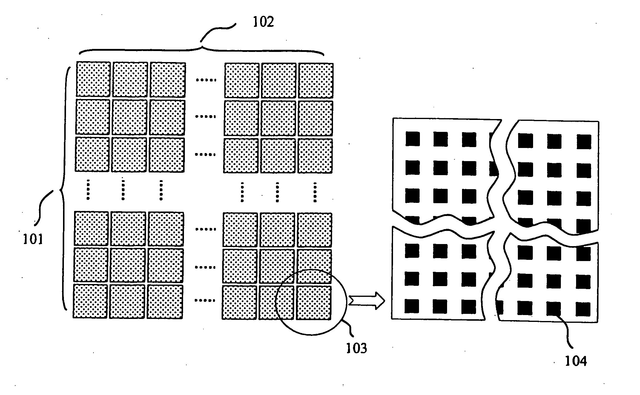
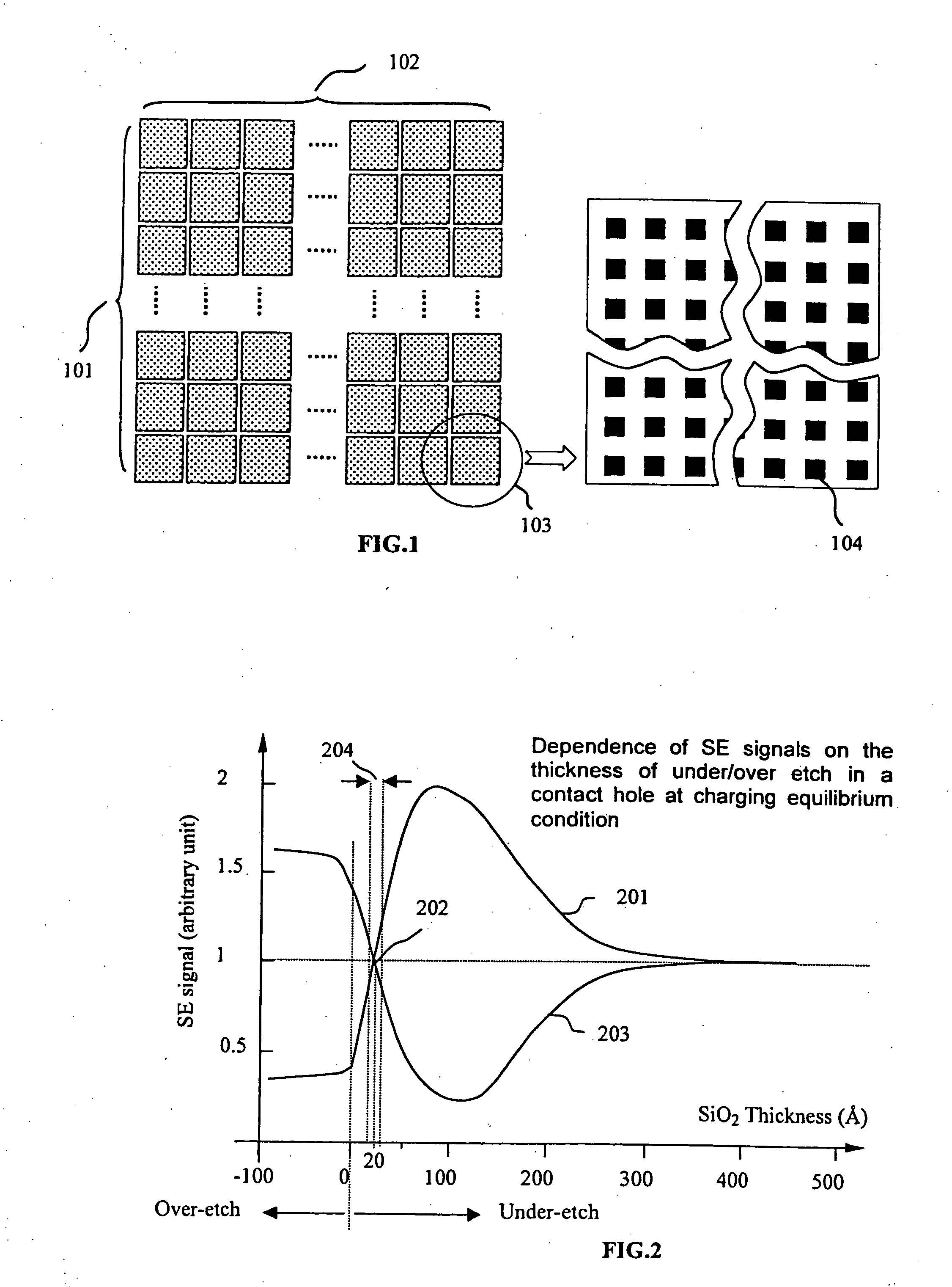
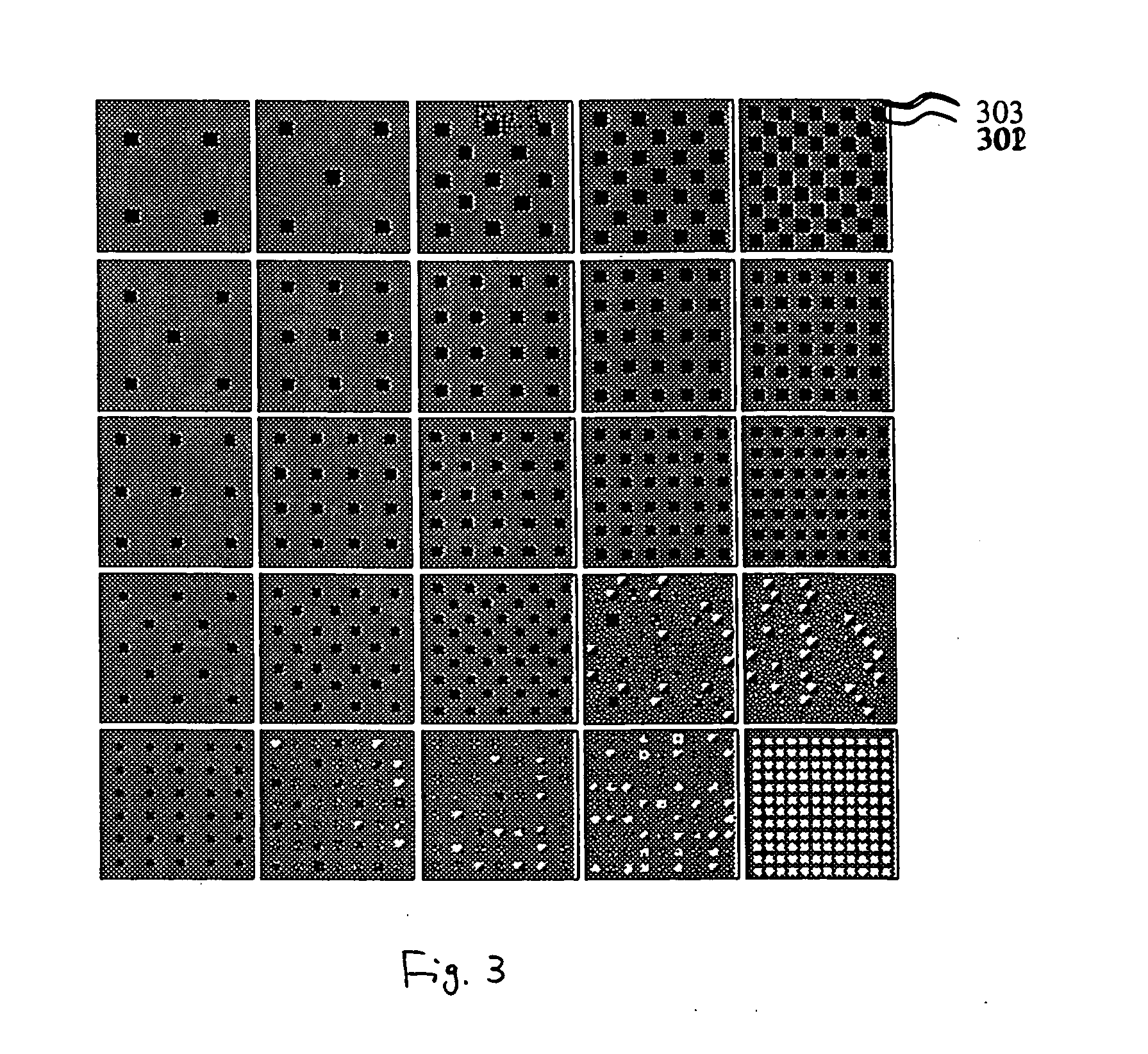
[0022]FIG. 1 depicts an embodiment of a via / contact test structure consisting of arrays 103 with increasing via / contact size along the row 101 direction and increasing densities or pattern factor (exposed Si area / wafer area) along the column 102 direction. Each via / contact array consists via / contact holes of a single size and density (pattern factor), as 104 indicates, and is etched simultaneously with the via / contacts in the functional dies into a dielectric layer of similar thickness and topography for making contact to the buried conductive layer or active regions such as source / drain. The aim of the embodiment is to have the etching process impose different etch rates, as the result of the microloading effect, and / or RIE lag, over the variant holes and to get uneven etch over the structure range from under-etch to over-etch. Other forms or modifications and / or embodiments may also meet this purpose and are thus intended to be covered by this disclosure. The embodiment of such te...


PUM


Abstract

A method for in-line monitoring of via/contact etching process based on a test structure is described. The test structure is comprised of via/contact holes of different sizes and densities in a layout such that, for a certain process, the microloading or RIE lag induced non-uniform etch rate produce under-etch in some regions and over-etch in others. A scanning electron microscope is used to distinguish these etching differences in voltage contrast images. Image processing and simple calibration convert these voltage contrast images into a “fingerprint” image characterizing the etching process in terms of thickness over-etched or under-etched. Tolerance of shifting or deformation of this image can be set for validating the process uniformity. This image can also be used as a measure to monitor long-term process parameter shifting, as well as wafer-to-wafer or lot-to-lot variations. Advanced process control (APC) can be performed in-line with the guidance of this image so that potential electrical defects are avoided and process yield ramp accelerated.

Description

CROSS REFERENCE TO RELATED APPLICATIONS [0001] This application is related to U.S. Provisional Application entitled “A Method For In-Line Monitoring Of Via / Contact Etching Process Uniformity In Semiconductor Wafer Manufacturing”, Application Number 60 / 329,917, filed Oct. 16, 2001. The prior application is hereby incorporated hereinto by reference. This application is also related to U.S. Provisional Application entitled “A Method For In-Line Monitoring Of Via / Contact Etching Process Uniformity In Semiconductor Wafer Manufacturing”, Application No. 60 / 332,016, filed Nov. 21, 2001.BACKGROUND OF THE INVENTION [0002] 1. Field of the Invention [0003] This invention relates generally to in-line monitoring of via / contact etching process in semiconductor device fabrication by using a scanning electron microscope (SEM), and more particularly to methods and devices for determining whether via / contact holes are over or under etched in the process of fabricating a semiconductor device. [0004] 2...

Claims


Application Information

Patent Timeline
IPC IPC(8): G01L21/30H01L21/44H01L21/66H01L21/768H01L23/544
CPCH01L21/76802H01L22/34H01L22/24
Inventor ZHAO, YANYEH, CHANG-CHUNCHEN, ZHONG-WEIJAU, JACK
Owner HERMES MICROVISION TAIWAN
Why Eureka
Try Eureka