Mounting structure

Inactive Publication Date: 2005-02-10
FUJITSU LTD
View PDF9 Cites 4 Cited by
  • Summary
  • Abstract
  • Description
  • Claims
  • Application Information

AI Technical Summary

Benefits of technology

[0029] In the first mounting structure, an electrically conductive sheet, e.g., a graphite sheet, having excellent thermal conductivity and exhibiting restorability and having a size identical with that of the base of the package is laid on the case at a package-bearing location, and the package and sheet are fastened together and attached to the case by two or more screws. In this case, the package is provided with fully open or half-open holes, the case is provided with screw holes, portions through which the screws are passed are made sheetless, and by fastening the package and sheet together by screws, the sheet is mounted on the case while the sheet is pressed by a pressing force of 10 N/cm2 or greater. In accordance with the first mounting structure, a rise in the temperature of the package can be suppressed through a simple method, a thermally excellent state can be obtained and electrical characteristics such as power application efficiency can be improved.
[0030] In a second mounting structure, in a case where steps are present between a package-bearing location and circuit-board-bearing location on the case, step portions, which are among step portions on four sides of the package-bearing location and through which microwaves do not pass, are inclined, an electrically conductive sheet having excellent thermal conductivity and exhibiting restorability is laid on the case on the entirety of the package- and circuit-board-bearing locations, and each of the package and circuit board and the sheet are fastened together and attached to the case by two or more screws. In this case, holes are provided in the sheet at portions through which the screws are passed, thereby resulting in a sheetless state, and by fastening the package and sheet together by screws, the sheet is mounted on the case while the sheet is pressed by a pressing force of 10 N/cm2 or greater. In accordance

Problems solved by technology

However, these expedients are applied to low-frequency circuits and are not implemented in the case of microwave circuits.
However, since a graphite sheet is not in liquid form as in the manner of grease, making it adhere perfectly is a difficult challenge.
Problems of mounting structures for microwave and millimeter-wave circuits
In particular, if the package bends due to heat, ground will not be stable and good electrical characteristics (microwave characteristics) will not be obtained.
Further, the heat-dissipating effect is limited, the package warps owing to evolution of heat and contact worsens, thus further destabilizing ground.
Even if grounding is achieved, the temperature of the semiconductor may exceed the absolute maximum rating if power consumption is high when one takes thermal resistance into account.
If the package is secured by soldering, however, it cannot be moved again.
The problem that arises is an increase in cost.
However, since the compound is an insulator, a problem encountered is that grounding is difficult to achieve.
In addition, the technique for applying the compound thinly and skillfully is difficult.
However, the sheet is squashed by pressure from above and has no resiliency.
If it is used for a long period of time, therefore, a gap may form between the package and the case.
This gives rise to reliability-related problems and a change in electrical characteristics.
However, it is difficult to apply the mounting structures of FIGS. 20 and 21 to mounting of a microwave circuit.
As a result, even if peripheral circuitry is installed, ground above the circuit is too close and it is difficult to obtain the usual microwave characteristics.
However, the existence of an adhesive layer enlarges thermal resistance.
Further, the lower part of the package of the transistor, MIC or MMIC used in a microwave and millimeter-wave band power circuit, which evolves a large amount of heat, is greater than 100° C. Since an adhesive layer can withstand a high temperature only on the order of 100° C., the sheet constituting the adhesive layer cannot be used in mounting a microwave circuit in the manner of the mounting structure of FIG. 21.
Further, since the mounting structure of FIG. 21 is for dealing with a low-frequency circuit, the special nature of microwave and millimeter-wave high-frequency circuits is not taken into consideration and there are limitations with regard to the mounting of a microwave circuit that requires the placement of a board, the principle part of which is a microstrip, in a surrounding area in close proximity to the package (transistor, MIC or MMIC).
As a result, even if circuitry is installed, ground above the circuit is too close and it is difficult to obtain the usual microwave and millimeter-wave characteristics.
However, this merely gives an assist in microwave and millimeter-wave applications and the package of a transistor, MIC or MMIC can

Method used


Image

  • Mounting structure
  • Mounting structure
  • Mounting structure

Examples


Example

(B) First Embodiment

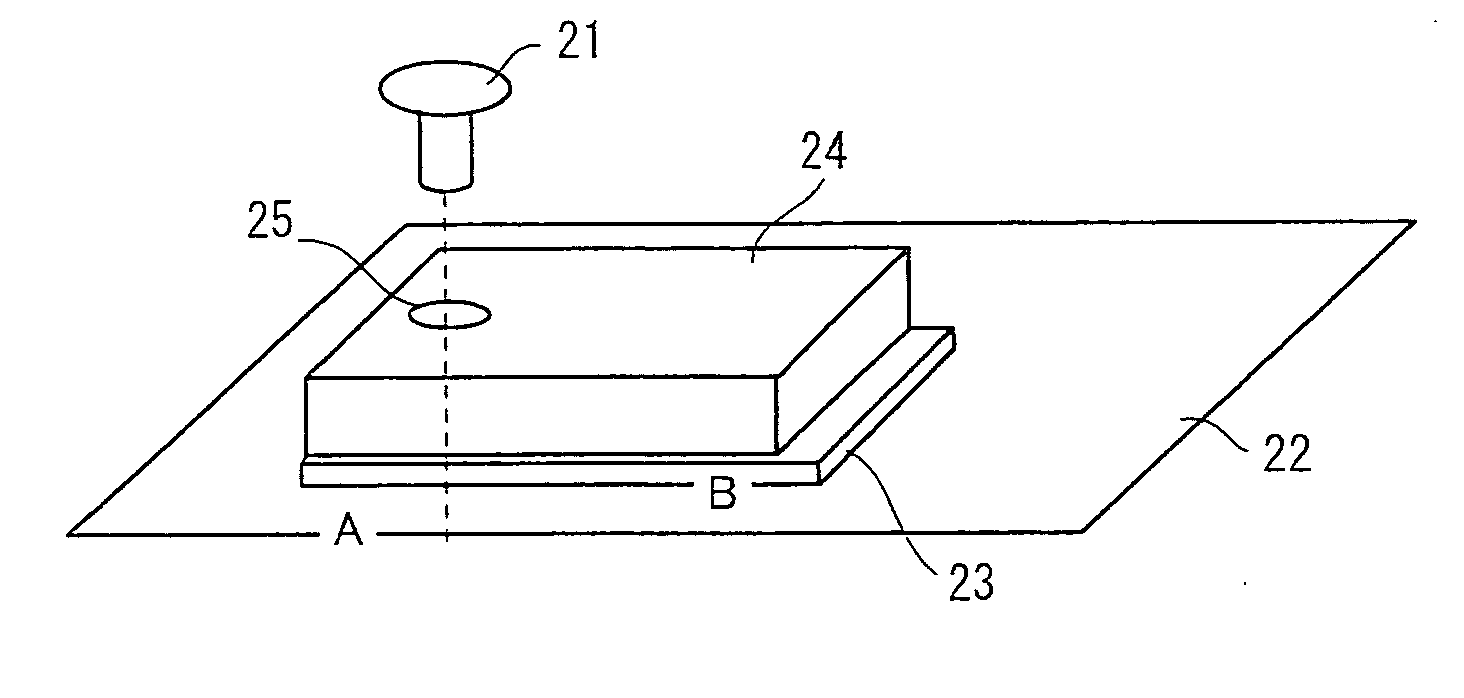
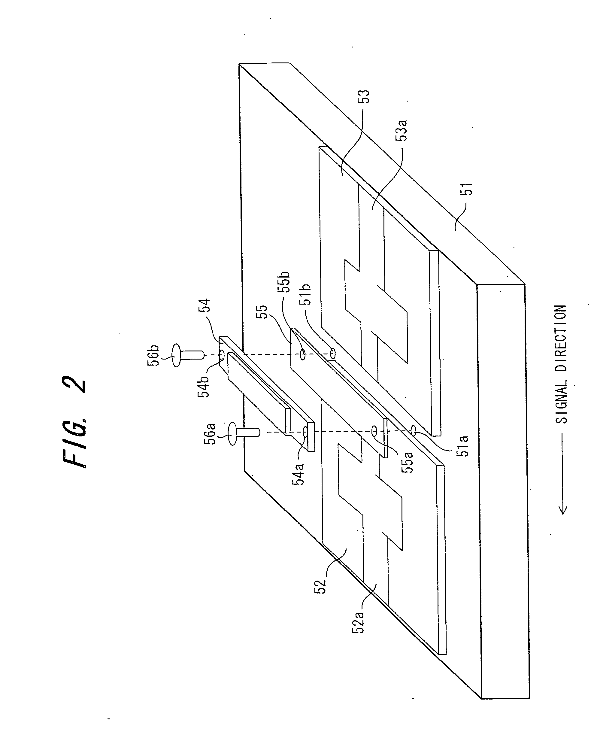
[0066]FIG. 2 is an exploded perspective view illustrating a package mounting structure according to a first embodiment, FIG. 3 a sectional view in case of sectioning along signal direction, and FIG. 4 a diagram for describing sizes of a package and graphite sheet. Circuit boards 52, 53 on which microstrips have been patterned are placed on a case (heat sink) 51, which serves as a heat-dissipating member, so as to sandwich a package 54 between them. Further, screw holes 51a, 51b for attaching the package are formed in the case 51.

[0067] The package 54 internally incorporates at least one of a high-frequency transistor, MIC and MMIC used in the microwave to-millimeter-wave band. The package has the external shape of a projection and the base portion thereof is formed at both ends to have holes 54a, 54b through which screws 56a, 56b for attaching the package are inserted. Further, packet input / output terminals 54c, 54d (not shown in FIG. 2; refer to FIG. 3) are fo...

Example

(C) Second Embodiment

[0079] In the first embodiment of FIG. 2, the case 51 is not formed to have a package accommodating portion and therefore positioning the sheet 55 and package 54 when the package is mounted is difficult. FIG. 14 is an exploded perspective view illustrating a package mounting structure according to a second embodiment, FIG. 15A is a sectional view taken along line AA′ when sectioning is performed along the signal direction, and FIG. 15B is a sectional view taken along line BB′ when sectioning is performed at right angles to the signal direction. Portions identical with those shown in FIGS. 2 and 3 are designated by like reference characters. This embodiment differs from the first embodiment in that the case 51 is formed to have a package accommodating portion 60. Providing the package accommodating portion 60 makes it possible to position the sheet 55 and package 54 in simple fashion merely by placing them in the accommodating portion 60 when the package is moun...

Example

(D) Third Embodiment

[0080] In the second embodiment, no problems whatsoever arise since a sheet having a size the same as that of the package base need only be set in the accommodating portion 60. However, there are cases where the sheet 55 is laid integrally on the case on the entirety of the locations that bear the package 54 and circuit boards 52, 53, and the package and circuit boards are grounded by the sheet. In such cases, right-angle steps 61 exist at four sides between the location that bears the package 54 and the locations that bear the circuit boards 52, 53, as evident from FIGS. 15A, 15B. Owing to the right-angle steps, the thin sheet 55 is severed by the right-angle portions of the steps 61 when the circuit boards 52, 53 are installed following the laying of the sheet and then the package 54 is set upon the sheet and is fastened by the screws 56a, 56b. Accordingly, in the third embodiment, if steps 61 exist between the package-bearing location and circuit-board-bearin...


PUM


Abstract

In a package mounting structure for mounting a package on a case, wherein the package internally incorporates at least one of a high-frequency transistor, MIC and MMIC used in the microwave to millimeter-wave band, and a base thereof is formed of metal and serves as ground, an electrically conductive sheet having excellent thermal conductivity and exhibiting restorability and having a size identical with that of the base of the package is laid on the case at a package-bearing location, the package and sheet are fastened together by two or more screws, and the sheet is mounted on the case while it is pressed by a pressing force of 10 N/cm2 or greater owing to fastening.

Description

BACKGROUND OF THE INVENTION [0001] This invention relates to a mounting structure of a package, which incorporates at least one of a high-frequency transformer, MIC (Microwave Integrated Circuit) and MMIC (Monolithic Microwave Integrated Circuit) used in the microwave to millimeter-wave band, or of a superconducting circuit board. More particularly, the invention relates to a mounting structure whereby a thermally excellent state can be obtained without sacrificing the microwave characteristic. [0002] Any of the following methods has been implemented heretofore in order to mount a microwave circuit, which handles signals in the microwave to millimeter-wave band, on a case (heat sink): {circumflex over (1)} the circuit is mounted upon interposing a soft metal such as indium between the case and the package or board; {circumflex over (2)} the circuit is mounted upon applying a silicon compound or grease between the case and the package or board; {circumflex over (3)} the circuit is mo...

Claims


Application Information

Patent Timeline
IPC IPC(8): H01L23/373H01L23/40H01L23/66H01L31/109H05K1/02H05K1/14H05K1/18
CPCH01L23/66H05K2201/10409H01L2223/6627H01L2924/1423H01L2924/15153H01L2924/15165H01L2924/1616H01L2924/16195H01L2924/16315H01L2924/166H01L2924/19032H05K1/0203H05K1/021H05K1/0243H05K1/142H05K1/182H05K3/0061H05K2201/0323H05K2201/09745H05K2201/10166H01L25/165
Inventor SHIGAKI, MASAFUMINAKAZAWA, ISAOYAMANAKA, KAZUNORI
Owner FUJITSU LTD
Why Eureka
Try Eureka