Distributed circular geometry power amplifier architecture

a technology of power amplifiers and circular geometry, applied in the direction of amplifiers with multiple amplifying elements, amplifiers with coupling networks, etc., can solve the problems of low resistance of lossy substrates, high cost, and high manufacturing difficulty of technologies, so as to reduce the loss, reduce the loss, and reduce the power loss

Inactive Publication Date: 2005-02-10
CALIFORNIA INST OF TECH
View PDF4 Cites 13 Cited by
  • Summary
  • Abstract
  • Description
  • Claims
  • Application Information

AI Technical Summary

Benefits of technology

[0019] The gain blocks that comprise the push-pull amplifiers used by the present invention may take various configurations, depending on the desired gain, circuit complexity, cost and other factors. In one basic embodiment, each gain block of each push-pull amplifier comprises a single three-terminal active device, such as a CMOS or bipolar transistor, having a cathode, an anode, and a control terminal. In another embodiment, each gain block of each push-pull amplifier comprises a compound device having at least a first and a last three-terminal active device. The active devices of each gain block are connected together in a cascoded fashion such that the cathode of the first active device serves as the negative terminal of the output port of each gain block, the anode of the last active device serves as the positive terminal of the output port of each gain block, and the control terminal of the first active device is the input port of the gain block. With this configuration, each push-pull amplifier, and thus the power amplifier, can advantageously supply more gain than can a single transistor per gain block design.
[0024] Furthermore, the secondary winding may advantageously comprise a single or multiple turn inductors formed by a variable width metal line. The metal line has sections that are relatively wide where a low ac voltage is present relative to the substrate and relatively narrow where a high ac voltage relative to the substrate is present. This geometry offers the advantage of further reducing the power loss, as it takes advantage of low metal resistance of wider metal where the ac voltage signal is low, thus reducing the loss and takes advantage of low capacitive coupling to the substrate of a narrower metal where the ac voltage is high, thus again reducing the loss. In this fashion, both the metal resistance loss and capacitive coupling loss are reduced
[0025] Turning momentarily back to the input circuit, the input power splitting network disclosed above may advantageously comprise a plurality of twisted input loops in proximity with the secondary winding, thereby providing magnetic coupling from the secondary winding. This geometry offers the advantage of further enhancing the gain or linearity of each push-pull amplifier in the power amplifier.
[0026] In yet a more detailed aspect of the preferred embodiment of the present invention, an additional secondary winding in proximity with and magnetically coupled to the primary and secondary windings may be provided to create an interdigitated transformer with its attendant benefits of lower power loss. Alternatively, or in addition to the multiple secondary winding improvement, the power amplifier of the present invention may further include at least one additional circular geometry primary winding in proximity with and magnetically coupled to the primary and secondary windings to create an interdigitated transformer.
[0029] Additionally described is a method for reducing the electrical losses of an inductor deposed on a substrate of an integrated circuit, the inductor have an elongated body with interconnected conducting sections, an average width and an average ac signal voltage across the body. The method includes decreasing the width of a section of the body of the inductor relative to the average width whereat the ac voltage signal on the section is relatively higher than the average ac signal voltage across the inductor body; and increasing the width of another section of the body of the inductor whereat the ac voltage signal on the other section is relatively lower than the average ac signal voltage across the inductor body.

Problems solved by technology

The design of high frequency power amplifiers with reasonable power levels, efficiency and gain remains one of the major challenges in the pursuit of a single-chip integrated transceiver.
For example, LDMOS transistors with a breakdown voltage of 20V have been used on a semi-insulating substrate, but still this design delivers only 200 mW.
Unfortunately, these technologies are significantly more costly and more difficult to manufacture than conventional silicon-based transistor technologies, such as CMOS.
Two significant problems in the design of a fully-integrated high speed solid state power amplifier using conventional silicon technologies such as CMOS are (1) the low resistivity of the lossy substrate which increases the loss of on-chip inductors and transformers; and (2) the low breakdown voltages of the transistors.
More particularly, the high conductivity of lossy substrates causes long metal lines, including conventional spiral inductors fabricated on the same substrate, to be very lossy in terms of power.
If the metal lines are made wide to reduce resistance, the capacitive coupling effect between the metal and substrate will drain part of the current to the substrate, thereby increasing power dissipation.
On the other hand, if the metal lines are made narrow enough to effectively overcome this problem, the metal resistance will significantly increase, again absorbing (dissipating) a significant portion of the power.
The low breakdown voltage of conventional transistors such as CMOS, for example, limits the maximum allowable drain voltage swing of the transistor.
While impedance transformation can be achieved using a 1:n transformer, unfortunately, an on-chip spiral 1:n transformer on a standard CMOS substrate is very lossy and will degrade the performance of the amplifier greatly.
Alternatively, an on-chip resonant match could be used, but this technique also results in significant power loss.
In sum, as all high frequency power amplifiers ostensibly require some inductors—essentially long metal lines—for matching purposes, connections for the supplies, and some form of power combining, conventional power amplifier circuits tend to be very power inefficient and not commercially viable above certain power and frequency levels.

Method used


Image

  • Distributed circular geometry power amplifier architecture
  • Distributed circular geometry power amplifier architecture
  • Distributed circular geometry power amplifier architecture

Examples


Embodiment Construction

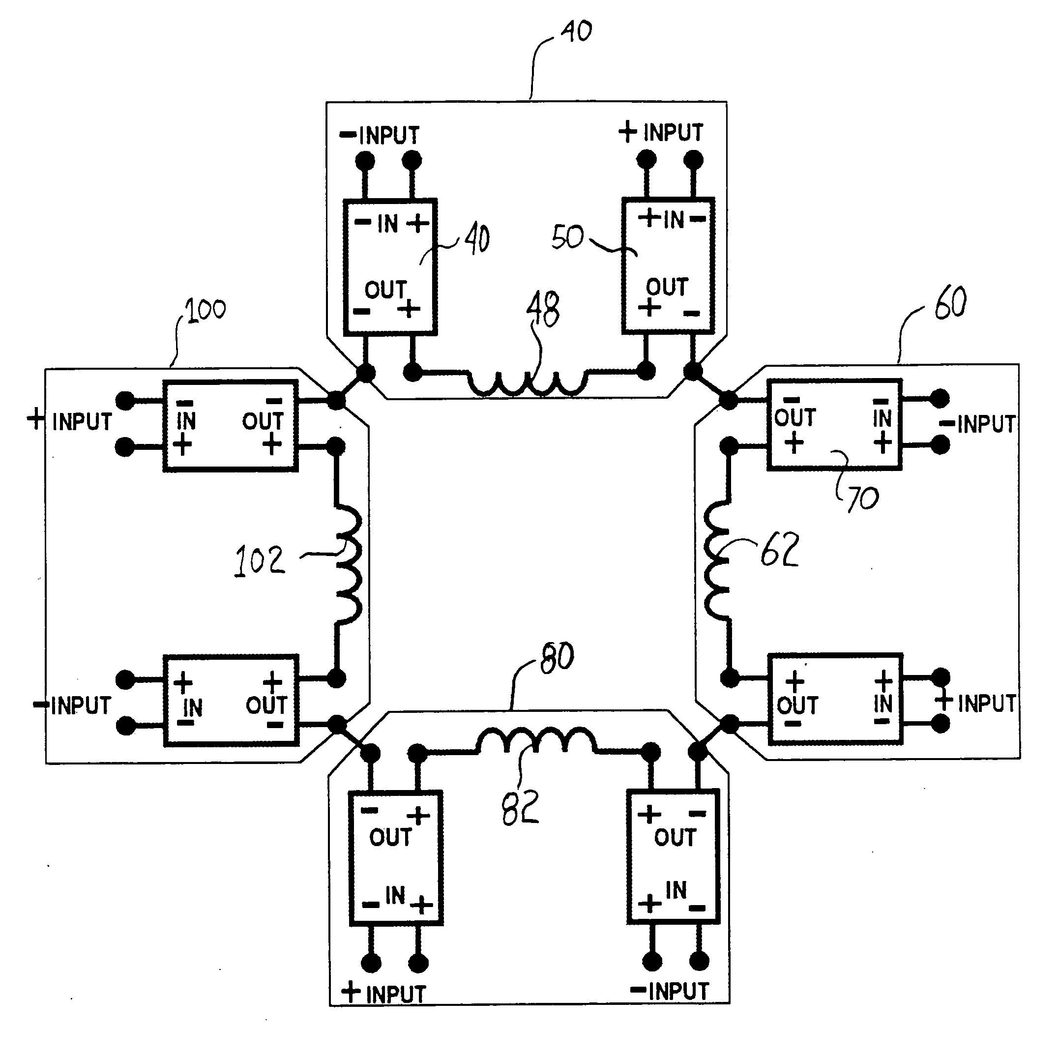
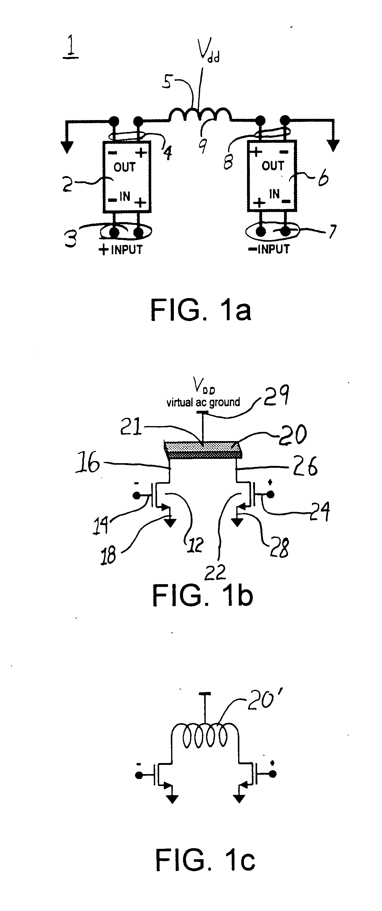
[0047] The present invention improves the performance and efficiency of high-frequency power amplifiers, especially for those used in modem communications devices and systems.

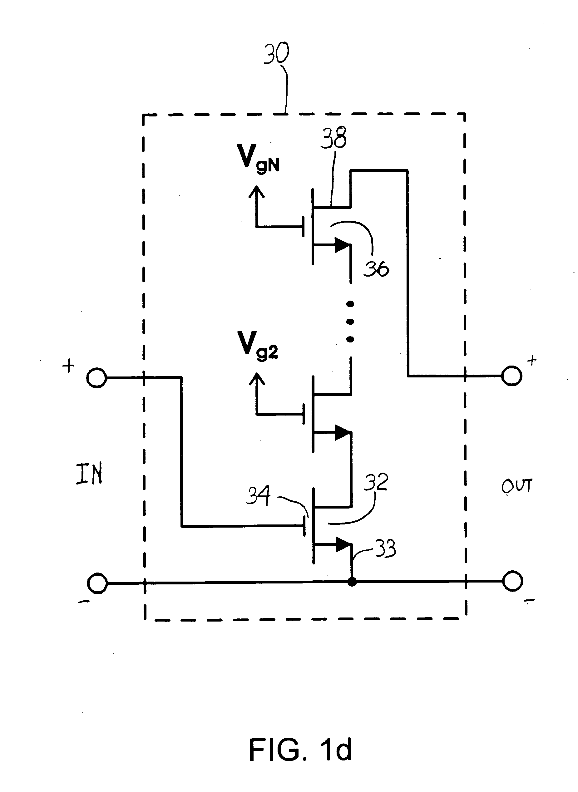
[0048] The present invention discloses novel combinations of three-terminal active devices used as amplifiers or switches or used as components of amplifiers or switches. The term “gain block” is used herein to generically describe any component or combination of components that is capable of providing gain. Thus, a gain block may include a single three-terminal active device, such as a transistor, or a combination thereof. The three terminals of an active device are herein referred to as the “control terminal,” the “anode”, and the “cathode,” corresponding, for example, to the gate, g, drain, d, and source, s, of a FET transistor, respectively, and corresponding to the base, collector, and emitter of a BJT transistor. Thus, these terms are to be understood in their broadest senses. Accordingly, the embodiment...


PUM


Abstract

The present invention discloses a distributed power amplifier topology and device that efficiently and economically enhances the power output of an RF signal to be amplified. The power amplifier comprises a plurality of push-pull amplifiers interconnected in a novel circular geometry that preferably function as a first winding of an active transformer having signal inputs of adjacent amplification devices driven with an input signal of equal magnitude and opposite phase. The topology also discloses the use of a secondary winding that matches the geometry of primary winding and variations thereof that serve to efficiently combine the power of the individual power amplifiers. The novel architecture enables the design of low-cost, fully-integrated, high-power amplifiers in the RF, microwave, and millimeter-wave frequencies.

Description

CROSS-REFERENCE TO RELATED APPLICATIONS [0001] This application claims the benefit of U.S. Provisional Application Nos. 60 / 239,470 and 60 / 239,474, both filed on Oct. 10, 2000 and U.S. Provisional Application No. 60 / 288,601, filed on May 4, 2001.BACKGROUND OF THE INVENTION [0002] 1. Field of the Invention [0003] The present invention relates to high frequency power amplifiers and more particularly to techniques for combining, monolithically or otherwise, individual power amplifiers to achieve power combining and impedance transformation. [0004] 2. Description of the Related Art [0005] The design of high frequency power amplifiers with reasonable power levels, efficiency and gain remains one of the major challenges in the pursuit of a single-chip integrated transceiver. Although several advances have been made in this direction, the design of a truly integrated power amplifier on a lossy substrate, such as silicon or silicon germanium has been an elusive goal. [0006] Multiple external...

Claims


Application Information

Patent Timeline
Patent Type & Authority Applications(United States)
IPC IPC(8): H03F1/22H03F3/26H03F3/42H03F3/60
CPCH03F1/223H03F3/265H03F3/423H03F2200/541H03F2200/534H03F2200/537H03F3/604H03F3/26
Inventor AOKI, ICHIROHAJIMIRI, SEYED-ALIRUTLEDGE, DAVID B.KEE, SCOTT DAVID
Owner CALIFORNIA INST OF TECH
Why Eureka
Try Eureka