Staggered in-situ deposition and etching of a dielectric layer for HDP CVD

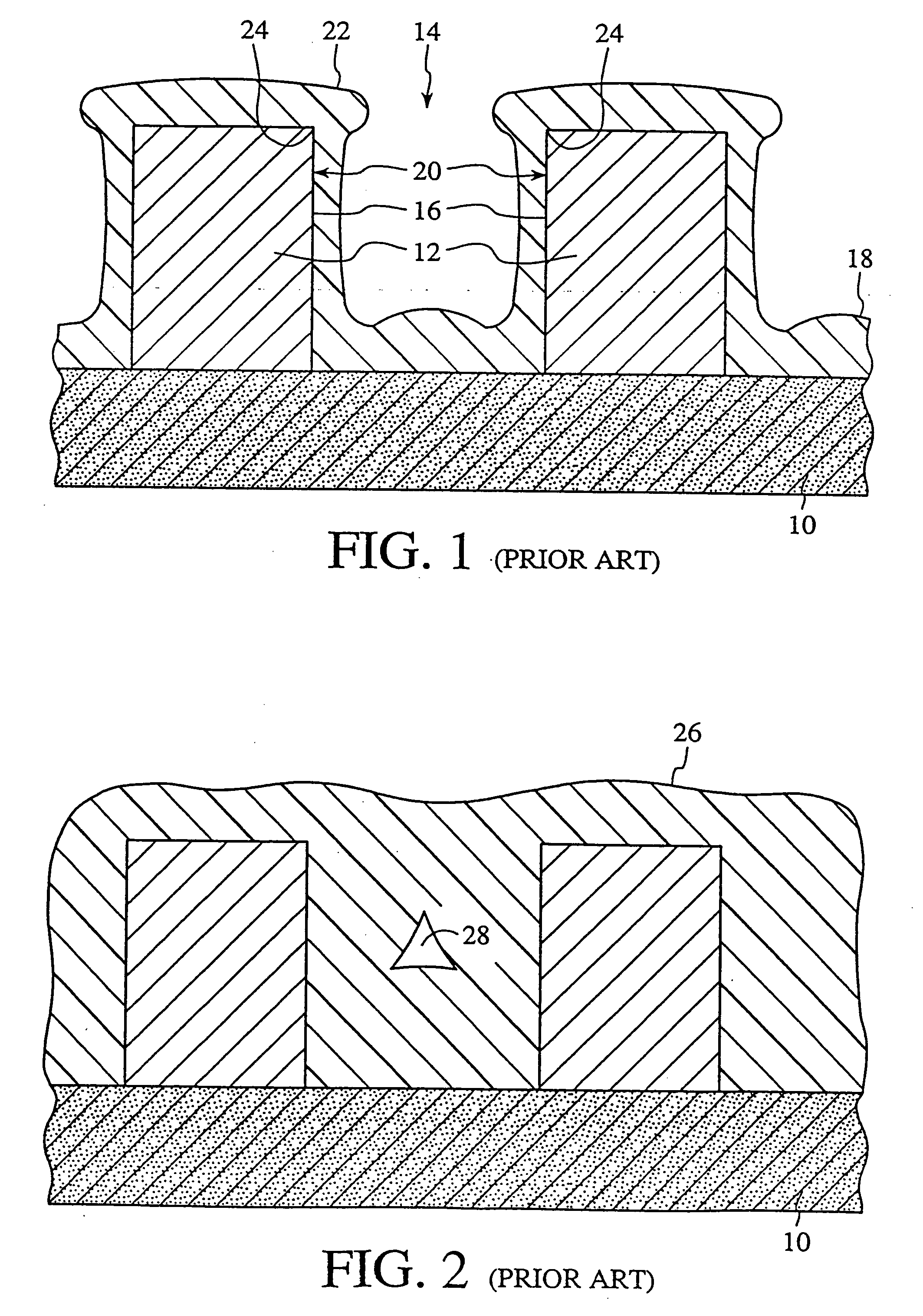
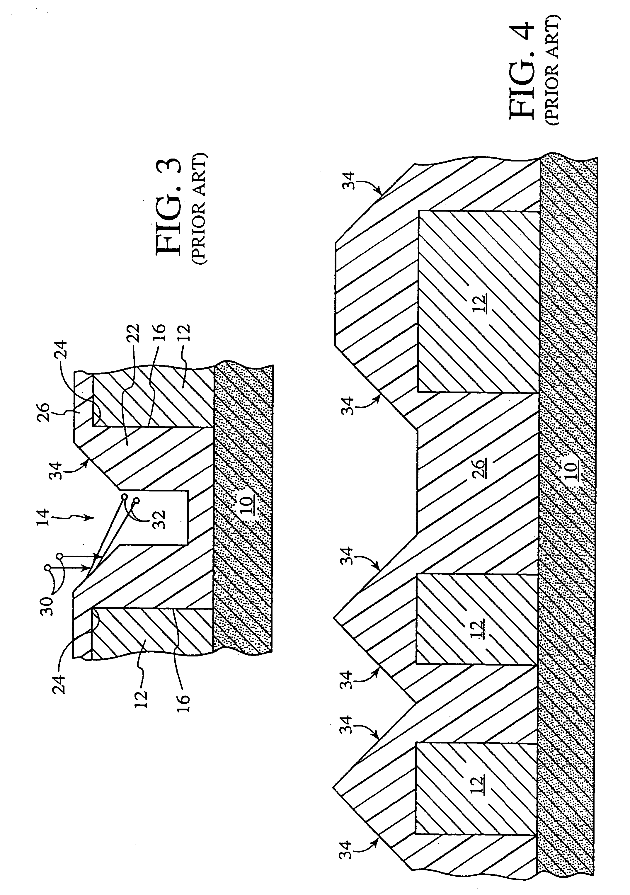
a dielectric layer and insitu deposition technology, applied in the direction of resistive material coating, superimposed coating process, liquid/solution decomposition chemical coating, etc., can solve the problem of difficult to completely fill the gap between adjacent conductive lines, the interior void 28 may be problematic for device fabrication, operation, reliability, etc., and the deposition rate available using conventional plasma cvd processes is still relatively low. , to achieve the effect of increasing the deposition rate of the conformal di

Inactive Publication Date: 2005-02-10
APPLIED MATERIALS INC
View PDF75 Cites 27 Cited by
  • Summary
  • Abstract
  • Description
  • Claims
  • Application Information

AI Technical Summary

Benefits of technology

The present invention provides a method and apparatus for greatly increasing the deposition rate of a conformal dielectric layer employing a dep-etch technique. The invention does so by selectively increasing inert gas source concentration, in a process chamber, without a significant increase in chamber pressure.
An important consideration during the dep-etch technique is that the deposition-to-etch ratio (dep-etch ratio) be maintained within a predetermined range so as to prevent over-etching and formation of interior voids. The present invention maintains the dep-etch ratio within a suitable range to prevent over-etch, while increasing the deposition rate of the dielectric layer to provide a 100% gap-fill of gaps having an aspect ratio up to 2.5:1. This is accomplished by rapidly increasing the etch rate of the dielectric layer, which allows increasing the deposition rate while maintaining a suitable dep-etch ratio. Specifically, it was discovered that the etch-rate of a dielectric layer is dependent not only upon the pressure of the process chamber, but also upon the concentration of the inert gas therein. The etch rate was found to be inversely proportional to the pressure in the process chamber and proportional to the concentration of inert gas present therein. By selectively terminating the flow of deposition gases in the process chamber, referred to as a staggered in-situ deposition technique, the pressure present therein may be decreased or maintained, while the inert gas concentration is substantially increased. In this fashion, the etch rate of the dielectric layer is substantially increased. The increased etch rate allows increasing the deposition rate using any deposition technique known to those skilled in the art. This decreases the time necessary to deposit the dielectric layer while maintaining a desired dep-etch ratio to provide the dielectric layer with superior gap-filling characteristics.

Problems solved by technology

One problem encountered, as the feature dimensions of the integrated circuits decrease, is that it becomes difficult to fill the gaps completely between adjacent conductive lines.
The interior void 28 may be problematic to device fabrication, operation, and reliability.
However, the deposition rates available using conventional plasma CVD processes are still relatively low.

Method used


Image

  • Staggered in-situ deposition and etching of a dielectric layer for HDP CVD
  • Staggered in-situ deposition and etching of a dielectric layer for HDP CVD
  • Staggered in-situ deposition and etching of a dielectric layer for HDP CVD

Examples


Embodiment Construction

I. Introduction

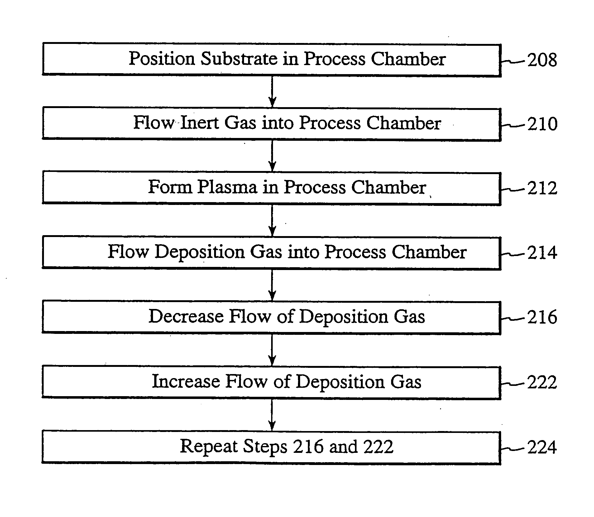
In one embodiment, a conformal dielectric layer formed from silicon dioxide is deposited on a stepped substrate employing a standard HDP-CVD system. A high deposition rate is achieved by selectively reducing the flow of deposition gases into a process chamber where a substrate having a stepped surface to be covered by the conformal dielectric layer is disposed. By selectively reducing the flow of deposition gases into the process chamber, the concentration of a sputtering gas, typically comprising argon, in the process chamber is increased without increasing the pressure therein. In this fashion, the etch rate of the conformal dielectric layer, having superior gap-filling characteristics, may be greatly increased to allow an increase in the deposition rate of the same, while maintaining a suitable dep-etch ratio.

II. An Exemplary CVD System

FIG. 5 illustrates one embodiment of a HDP-CVD system 36, in which a dielectric layer according to the present invention can be...


PUM

PropertyMeasurementUnit
pressureaaaaaaaaaa
pressureaaaaaaaaaa
sizeaaaaaaaaaa

Abstract

A method and apparatus for depositing a conformal dielectric layer employing a dep-etch technique features selectively reducing the flow of deposition gases into a process chamber where a substrate having a stepped surface to be covered by the conformal dielectric layer is disposed. By selectively reducing the flow of deposition gases into the process chamber, the concentration of a sputtering gas, from which a plasma is formed, in the process chamber is increased without increasing the pressure therein. It is preferred that the flow of deposition gases be periodically terminated so as to provide a sputtering gas concentration approaching 100%. In this fashion, the etch rate of a conformal dielectric layer having adequate gap-filling characteristics may be greatly increased, while allowing an increase in the deposition rate of the same.

Description

BACKGROUND OF THE INVENTION The present invention relates to the fabrication of integrated circuits. More particularly, the present invention is directed toward a method and apparatus for increasing the deposition rate of a conformal dielectric layer, having excellent gap-filling characteristics, deposited over a stepped surface. Semiconductor device geometries continue to decrease in size, providing more devices per unit area on a fabricated wafer. Currently, some devices are fabricated with feature dimensions as small as 0.18 μm. For example, spacing between conductive lines or traces on a patterned wafer may be separated by 0.18 μm leaving recesses or gaps of a comparable size. A nonconductive layer of dielectric material, such as silicon dioxide, is typically deposited over the features to fill the aforementioned gap and insulate the features from other features of the integrated circuit in adjacent layers or from adjacent features in the same layer. One problem encountered, ...

Claims


Application Information

Patent Timeline
Patent Type & Authority Applications(United States)
IPC IPC(8): C23C16/04C23C16/40C23C16/44C23C16/455H01J37/32H01L21/302H01L21/3065H01L21/31H01L21/3105H01L21/316H01L21/768
CPCC23C16/045H01L21/76837C23C16/4482C23C16/45523C23C16/45561C23C16/507H01J37/321H01J37/32302H01J37/32449H01J37/32862H01J37/3299H01L21/02164H01L21/02211H01L21/02274H01L21/31051H01L21/31608H01L21/31612C23C16/402C23C16/40
Inventor ROSSMAN, KENT
Owner APPLIED MATERIALS INC
Why Eureka
Try Eureka